SNVS353F February 2005 – September 2016 LM2753
PRODUCTION DATA.
- 1 Features
- 2 Applications
- 3 Description
- 4 Revision History
- 5 Pin Configuration and Functions
- 6 Specifications
- 7 Detailed Description
- 8 Application and Implementation
- 9 Power Supply Recommendations
- 10Layout
- 11Device and Documentation Support
- 12Mechanical, Packaging, and Orderable Information
Package Options
Mechanical Data (Package|Pins)
- DSC|10
Thermal pad, mechanical data (Package|Pins)
- DSC|10
Orderable Information
6 Specifications
6.1 Absolute Maximum Ratings
over operating free-air temperature range (unless otherwise noted)(1)(2)| MIN | MAX | UNIT | ||
|---|---|---|---|---|
| VIN pin: voltage to GND | –0.3 | 6 | V | |
| EN, FLASH pins: voltage to GND | –0.3 | (VIN + 0.3) w/ 6 V maximum | V | |
| Continuous power dissipation(3) | Internally limited | |||
| Junction temperature, TJ-MAX-ABS | 150 | °C | ||
| Storage temperature, Tstg | −65 | 150 | °C | |
(1) Stresses beyond those listed under Absolute Maximum Ratings may cause permanent damage to the device. These are stress ratings only, which do not imply functional operation of the device at these or any other conditions beyond those indicated under Recommended Operating Conditions. Exposure to absolute-maximum-rated conditions for extended periods may affect device reliability.
(2) All voltages are with respect to the potential at the GND pin.
(3) In applications where high power dissipation and/or poor package thermal resistance is present, the maximum ambient temperature may have to be derated. Maximum ambient temperature (TA-MAX) is dependent on the maximum operating junction temperature (TJ-MAX-OP = 120°C), the maximum power dissipation of the device in the application (PD-MAX), and the junction-to ambient thermal resistance of the part/package in the application (RθJA), as given by the following equation: TA-MAX = TJ-MAX-OP – (RθJA × PD-MAX).
6.2 ESD Ratings
| VALUE | UNIT | |||
|---|---|---|---|---|
| V(ESD) | Electrostatic discharge | Human-body model (HBM), per ANSI/ESDA/JEDEC JS-001(1) | ±2000 | V |
| Machine model | ±200 | |||
(1) JEDEC document JEP155 states that 500-V HBM allows safe manufacturing with a standard ESD control process.
6.3 Recommended Operating Conditions
over operating free-air temperature range (unless otherwise noted)(2)| MIN | MAX | UNIT | ||
|---|---|---|---|---|
| Input voltage | 3 | 5.5 | V | |
| EN, FLASH input voltage | 0 | VIN | V | |
| Junction temperature, TJ | –40 | 120 | °C | |
| Ambient temperature, TA(3) | –40 | 85 | °C | |
6.4 Thermal Information
| THERMAL METRIC(1) | LM2753 | UNIT | |
|---|---|---|---|
| DSC (WSON) | |||
| 10 PINS | |||
| RθJA | Junction-to-ambient thermal resistance | 52.5 | °C/W |
| RθJC(top) | Junction-to-case (top) thermal resistance | 63.0 | °C/W |
| RθJB | Junction-to-board thermal resistance | 27.2 | °C/W |
| ψJT | Junction-to-top characterization parameter | 0.9 | °C/W |
| ψJB | Junction-to-board characterization parameter | 27.3 | °C/W |
| RθJC(bot) | Junction-to-case (bottom) thermal resistance | 7.3 | °C/W |
(1) For more information about traditional and new thermal metrics, see Semiconductor and IC Package Thermal Metrics.
6.5 Electrical Characteristics
Unless otherwise noted, specifications apply to the Simplified Schematic with TA = 25°C, VIN = 3.6 V, V(EN) = VIN,V(FLASH) = GND, C1 = 1 µF, CIN = COUT = 10 µF.(1) (2).
| PARAMETER | TEST CONDITIONS | MIN | TYP | MAX | UNIT | |
|---|---|---|---|---|---|---|
| VOUT | Output voltage | 3 V ≤ VIN ≤ 5.5 V, IOUT ≤ 100 mA | 5 | V | ||
| 3 V ≤ VIN ≤ 5.5 V, IOUT ≤ 100 mA –40°C ≤ TA ≤ 85°C |
4.75 (–5%) | 5.25 (5%) | ||||
| IVOUT | Continuous load current | 3 V ≤ VIN ≤ 5.5 V, VOUT = 5 V (typical) | 200 | mA | ||
| IOUT | Pulsed flash current | V(FLASH) = 1.8 V, TPULSE = 500 ms VIOUT-MAX = 4.1 V (typical) |
400 | mA | ||
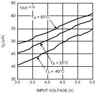
| IQ | Quiescent current | IOUT = 0 mA, 3 V ≤ VIN ≤ 5.5 V | 60 | µA | ||
| IOUT = 0 mA, 3 V ≤ VIN ≤ 5.5 V –40°C ≤ TA ≤ 85°C |
80 | |||||
| ISD | Shutdown supply current | V(EN) = 0 V 3 V ≤ VIN ≤ 5.5 V |
0.1 | 1 | µA | |
| V(EN) = 0 V, 3 V ≤ VIN ≤ 5.5 V TA = 85°C |
0.2 | |||||
| ROUT | Output impedance | VIN = 3.2 V | 5.3 | Ω | ||
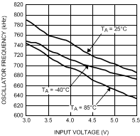
| ƒSW | Switching frequency | 3 V ≤ VIN ≤ 5.5 V | 725 | kHz | ||
| 3 V ≤ VIN ≤ 5.5 V, –40°C ≤ TA ≤ 85°C | 475 | 950 | ||||
| VIH | Logic input high | Input pins: EN, FLASH, –40°C ≤ TA ≤ 85°C | 1.2 | VIN | V | |
| VIL | Logic input low | Input pins: EN, FLASH, –40°C ≤ TA ≤ 85°C | 0 | 0.3 | V | |
| IIH | Logic input high current | V(EN) = V(FLASH) = 3 V | 10 | µA | ||
| IIL | Logic input low current | V(EN) = V(FLASH) = 0 V | 10 | nA | ||
| tON | Turnon time(3) | 640 | µs | |||
| tFLASH | Flash turnon time(4) | V(FLASH) = 3.6 V | 10 | ns | ||
(1) Minimum (MIN) and maximum (MAX) limits are specified by design, test, or statistical analysis. Typical (TYP) numbers are not specified, but represent the most likely norm.
(2) CIN, COUT, and C1: Low-ESR surface-mount ceramic capacitors (MLCCs) are used in setting electrical characteristics.
(3) Turnon time is measured from when the EN signal is pulled high until the output voltage on VOUT crosses 90% of its final value.
(4) Flash turnon time is measured from when the FLASH signal is pulled high until the voltage on IOUT crosses 90% of its final programmed value.
6.6 Typical Characteristics
Unless otherwise specified: TA = 25°C, VIN = 3.6 V, V(FLASH) = GND, V(EN) = VIN, CIN = COUT = 10 µF, C1 = 1 µF.
