SNVS551E April 2008 – May 2016 LM2758
PRODUCTION DATA.
- 1 Features
- 2 Applications
- 3 Description
- 4 Revision History
- 5 Pin Configuration and Functions
- 6 Specifications
- 7 Detailed Description
- 8 Application and Implementation
- 9 Power Supply Recommendations
- 10Layout
- 11Device and Documentation Support
- 12Mechanical, Packaging, and Orderable Information
Package Options
Mechanical Data (Package|Pins)
- YZR|12
Thermal pad, mechanical data (Package|Pins)
Orderable Information
5 Pin Configuration and Functions
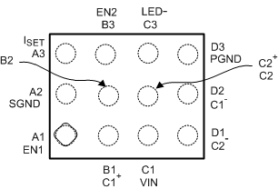
YZR Package
12-Pin DSBGA
Top View

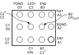
YZR Package
12-Pin DSBGA
Bottom View

Pin Functions
| PIN | TYPE | DESCRIPTION | |
|---|---|---|---|
| NO. | NAME | ||
| A1 | EN1 | Input | The EN2 pins is used to select the modes (torch, indicator, flash), as well as to put the part into shutdown mode. |
| A2 | SGND | Ground | Analog and control ground for charge pump. Connect this pin directly to a low impedance ground plane. |
| A3 | ISET | Power | LED current programming resistor pin. A resistor connected between this pin, and GND is used to set torch, flash and indicator currents. |
| B1 | C1+ | Power | Flying capacitor pin — connect a 1-µF ceramic capacitor from C1+ to C1− |
| B2 | CPOUT | Output | Charge pump regulated output. A 2.2-µF ceramic capacitor is required from CPOUT to GND. Connect flash LED anode to this pin. |
| B3 | EN2 | Input | The EN1 pin is used to select the modes (torch, indicator, flash), as well as to put the part into Shutdown mode. |
| C1 | VIN | Input | Supply voltage connection |
| C2 | C2+ | Power | Flying capacitor pins — connect a 1-µF ceramic capacitor from C2+ to C2−. |
| C3 | LED− | Output | Regulated current source output. Connect flash LED cathode to this pin. |
| D1 | C2− | Power | Flying capacitor pin — connect a 1-µF ceramic capacitor from C2+ to C2−. |
| D2 | C1− | Power | Flying capacitor pin — connect a 1-µF ceramic capacitor from C1+ to C1− |
| D3 | PGND | Ground | Power ground for the charge pump and the current source. Connected the pin directly to a low-impedance ground plane. |