SNVS069E February   2000  – January 2022 LM2767

PRODUCTION DATA  

  1. Features
  2. Applications
  3. Description
  4. Revision History
  5. Pin Configuration and Functions
  6. Specifications
    1. 6.1 Absolute Maximum Ratings
    2. 6.2 ESD Ratings
    3. 6.3 Recommended Operating Conditions
    4. 6.4 Thermal Information
    5. 6.5 Electrical Characteristics
    6. 6.6 Typical Characteristics
  7. Parameter Measurement Information
    1. 7.1 Test Circuit
  8. Detailed Description
    1. 8.1 Overview
    2. 8.2 Functional Block Diagram
    3. 8.3 Feature Description
    4. 8.4 Device Functional Modes
  9. Application and Implementation
    1. 9.1 Application Information
    2. 9.2 Typical Application
      1. 9.2.1 Design Requirements
      2. 9.2.2 Detailed Design Procedure
        1. 9.2.2.1 Positive Voltage Doubler
        2. 9.2.2.2 Capacitor Selection
        3. 9.2.2.3 Paralleling Devices
        4. 9.2.2.4 Cascading Devices
        5. 9.2.2.5 Regulating VOUT
      3. 9.2.3 Application Curve
  10. 10Power Supply Recommendations
  11. 11Layout
    1. 11.1 Layout Guidelines
    2. 11.2 Layout Example
  12. 12Device and Documentation Support
    1. 12.1 Device Support
      1. 12.1.1 Third-Party Products Disclaimer
    2. 12.2 Receiving Notification of Documentation Updates
    3. 12.3 Support Resources
    4. 12.4 Trademarks
    5. 12.5 Electrostatic Discharge Caution
    6. 12.6 Glossary
  13. 13Mechanical, Packaging, and Orderable Information

Package Options

Mechanical Data (Package|Pins)
Thermal pad, mechanical data (Package|Pins)
Orderable Information

Paralleling Devices

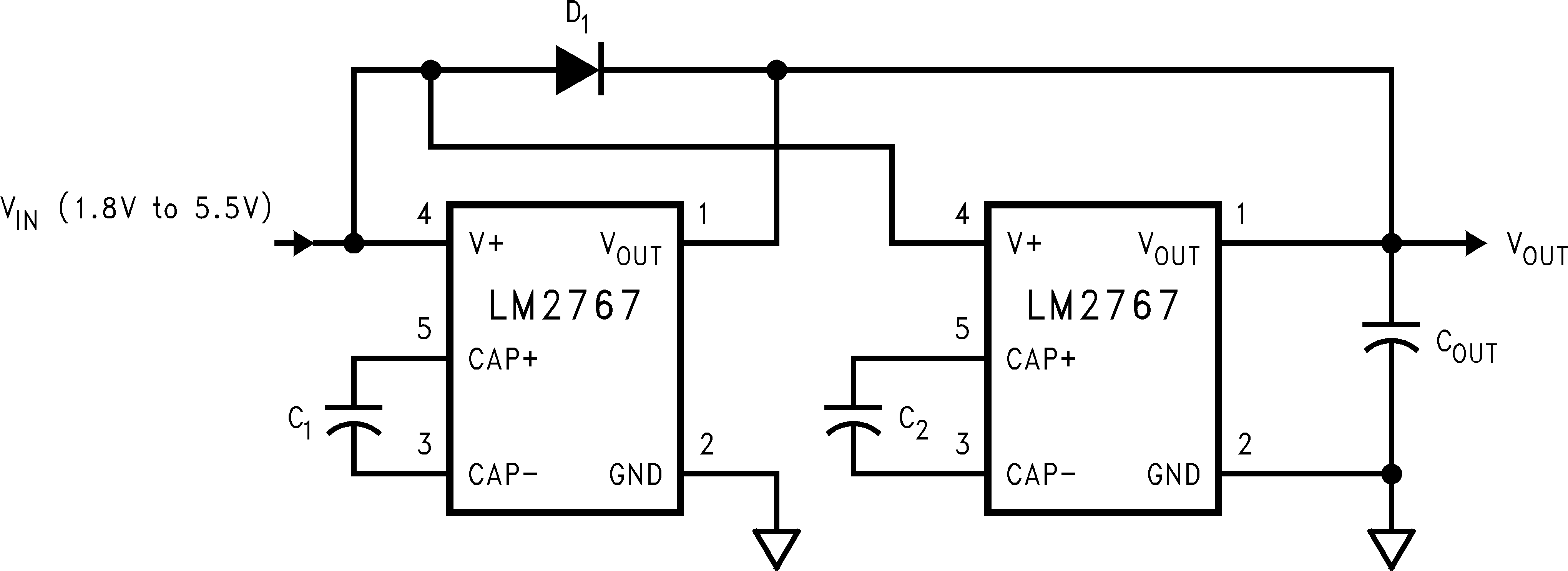
Any number of LM2767 devices can be paralleled to reduce the output resistance. Because there is no closed loop feedback, as found in regulated circuits, stable operation is assured. Each device must have its own pumping capacitor C1, while only one output capacitor COUT is needed as shown in Figure 9-3. The composite output resistance is:

Equation 4. GUID-16240FA8-2660-402D-AD32-A521CB4D8148-low.gif
GUID-DE2F0463-759D-46CC-A04C-B649E95D4F3B-low.pngFigure 9-3 Lowering Output Resistance by Paralleling Devices