SNVSA85C October   2015  – January 2017 LM27761

PRODUCTION DATA.  

  1. Features
  2. Applications
  3. Description
    1.     Device Images
      1.      Typical Application
  4. Revision History
  5. Pin Configuration and Functions
    1.     Pin Functions
  6. Specifications
    1. 6.1 Absolute Maximum Ratings
    2. 6.2 ESD Ratings
    3. 6.3 Recommended Operating Conditions
    4. 6.4 Thermal Information
    5. 6.5 Electrical Characteristics
    6. 6.6 Typical Characteristics
  7. Detailed Description
    1. 7.1 Overview
    2. 7.2 Functional Block Diagram
    3. 7.3 Feature Description
      1. 7.3.1 Undervoltage Lockout
      2. 7.3.2 Input Current Limit
      3. 7.3.3 PFM Operation
      4. 7.3.4 Output Discharge
      5. 7.3.5 Thermal Shutdown
    4. 7.4 Device Functional Modes
      1. 7.4.1 Shutdown Mode
      2. 7.4.2 Enable Mode
  8. Application and Implementation
    1. 8.1 Application Information
    2. 8.2 Typical Application - Regulated Voltage Inverter
      1. 8.2.1 Design Requirements
      2. 8.2.2 Detailed Design Procedure
        1. 8.2.2.1 Custom Design With WEBENCH® Tools
        2. 8.2.2.2 Charge-Pump Voltage Inverter
        3. 8.2.2.3 Negative Low-Dropout Linear Regulator
        4. 8.2.2.4 Power Dissipation
        5. 8.2.2.5 Output Voltage Setting
        6. 8.2.2.6 External Capacitor Selection
          1. 8.2.2.6.1 Charge-Pump Output Capacitor
          2. 8.2.2.6.2 Input Capacitor
          3. 8.2.2.6.3 Flying Capacitor
          4. 8.2.2.6.4 LDO Output Capacitor
      3. 8.2.3 Application Curves
  9. Power Supply Recommendations
  10. 10Layout
    1. 10.1 Layout Guidelines
    2. 10.2 Layout Example
  11. 11Device and Documentation Support
    1. 11.1 Device Support
      1. 11.1.1 Development Support
        1. 11.1.1.1 Custom Design With WEBENCH® Tools
    2. 11.2 Receiving Notification of Documentation Updates
    3. 11.3 Community Resources
    4. 11.4 Trademarks
    5. 11.5 Electrostatic Discharge Caution
    6. 11.6 Glossary
  12. 12Mechanical, Packaging, and Orderable Information

Package Options

Mechanical Data (Package|Pins)
Thermal pad, mechanical data (Package|Pins)
Orderable Information

Typical Characteristics

Unless otherwise specified, TA = 25°C, VIN = 5 V, and values for C1 to C4 are as shown in theTypical Application.
LM27761 D001_SNVSA85.gif
Figure 1. Output Voltage Ripple vs Output Current
LM27761 D015_SNVSA85.gif
EN = 1 ILOAD = 0 mA
Figure 3. Quiescent Current
LM27761 D006_SNVSA85.gif
VIN = 3 V VOUT = –1.8 V
R1 = 237 kΩ R2 = 500 kΩ
Figure 5. Load Regulation
LM27761 D011_SNVSA85.gif
VIN = 5 V VOUT = –3.3 V
R1 = 856 kΩ R2 = 500 kΩ
Figure 7. Load Regulation
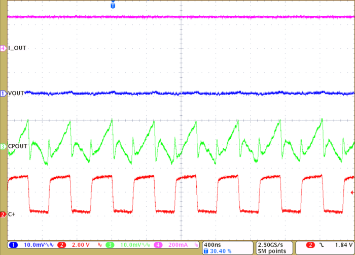
LM27761 wvfrm02_output_voltage_ripple_5p0v_snvsa85.png
VIN = 5.5 V VOUT = –5 V IOUT = 250 mA
Figure 9. Output Voltage Ripple
LM27761 wvfrm04_enable_low_snvsa85.png
Figure 11. Enable Low
LM27761 D012_SNVSA85.gif
VOUT = –1.8 V IOUT = 50 mA
R1 = 237 kΩ R2 = 500 kΩ
Figure 13. Line Regulation
LM27761 D014_SNVSA85.gif
VOUT = –1.8 IOUT = 250 mA R1 = 237 kΩ R2 = 500 kΩ
Figure 15. Line Regulation
LM27761 D002_SNVSA85.gif
VOUT = –1.8 V IOUT = 100 mA
Figure 2. Output Voltage Ripple vs Input Voltage
LM27761 D016_SNVSA85.gif
EN = 0
Figure 4. Shutdown Current
LM27761 D007_SNVSA85.gif
VIN = 5.5 V VOUT = –5 V
R1 = 1.54 MΩ R2 = 500 kΩ
Figure 6. Load Regulation
LM27761 wvfrm01_output_voltage_ripple_1p8v_snvsa85.png
VIN = 3 V VOUT = –1.8 V IOUT = 250 mA
Figure 8. Output Voltage Ripple
LM27761 wvfrm03_enable_high_snvsa85.png
Figure 10. Enable High
LM27761 D008_SNVSA85.gif
Figure 12. LDO Dropout Voltage vs IOUT
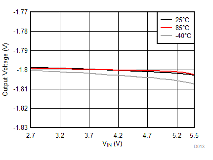
LM27761 D013_SNVSA85.gif
VOUT = –1.8 V IOUT = 100 mA
R1 = 237 kΩ R2 = 500 kΩ
Figure 14. Line Regulation