SNVSBE5 April   2019 LM2840-Q1 , LM2841-Q1 , LM2842-Q1

PRODUCTION DATA.  

  1. Features
  2. Applications
  3. Description
    1.     Device Images
      1.      Typical Application Circuit
  4. Revision History
  5. Pin Configuration and Functions
    1.     Pin Functions
  6. Specifications
    1. 6.1 Absolute Maximum Ratings
    2. 6.2 ESD Ratings
    3. 6.3 Recommended Operating Conditions
    4. 6.4 Thermal Information
    5. 6.5 Electrical Characteristics
    6. 6.6 Typical Characteristics
  7. Detailed Description
    1. 7.1 Overview
    2. 7.2 Functional Block Diagram
    3. 7.3 Feature Description
      1. 7.3.1 Protection
    4. 7.4 Device Functional Modes
      1. 7.4.1 Continuous Conduction Mode
  8. Application and Implementation
    1. 8.1 Application Information
    2. 8.2 Typical Applications
      1. 8.2.1 Design Requirements
      2. 8.2.2 Detailed Design Procedure
        1. 8.2.2.1 Custom Design With WEBENCH® Tools
        2. 8.2.2.2 Setting the Output Voltage
        3. 8.2.2.3 Inductor Selection
        4. 8.2.2.4 Input Capacitor
        5. 8.2.2.5 Output Capacitor
        6. 8.2.2.6 Bootstrap Capacitor
        7. 8.2.2.7 Soft-Start Components
        8. 8.2.2.8 Shutdown Operation
        9. 8.2.2.9 Schottky Diode
      3. 8.2.3 Application Curves
      4. 8.2.4 Other Application Circuits
  9. Power Supply Recommendations
  10. 10Layout
    1. 10.1 Layout Guidelines
    2. 10.2 Layout Example
  11. 11Device and Documentation Support
    1. 11.1 Device Support
      1. 11.1.1 Third-Party Products Disclaimer
      2. 11.1.2 Development Support
        1. 11.1.2.1 Custom Design With WEBENCH® Tools
    2. 11.2 Documentation Support
      1. 11.2.1 Related Documentation
    3. 11.3 Related Links
    4. 11.4 Receiving Notification of Documentation Updates
    5. 11.5 Community Resources
    6. 11.6 Trademarks
    7. 11.7 Electrostatic Discharge Caution
    8. 11.8 Glossary
  12. 12Mechanical, Packaging, and Orderable Information

Package Options

Mechanical Data (Package|Pins)
Thermal pad, mechanical data (Package|Pins)
Orderable Information

Other Application Circuits

Figure 13 to Figure 16 show application circuit examples using the LM284x-Q1 devices. Customers must fully validate and test these circuits before implementing a design based on these examples. Unless otherwise noted, the design procedures in are applicable to these designs.

LM2840-Q1 LM2841-Q1 LM2842-Q1 30036708.gifFigure 13. Step-Down Converter With 5-V Output Voltage
LM2840-Q1 LM2841-Q1 LM2842-Q1 30036709.gifFigure 14. Step-Down Converter With 12-V Output Voltage
LM2840-Q1 LM2841-Q1 LM2842-Q1 30036716.gifFigure 15. Step-Down Converter With 15-V Output Voltage
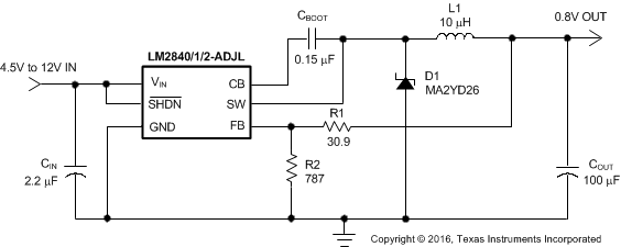
LM2840-Q1 LM2841-Q1 LM2842-Q1 30036717.gifFigure 16. Step-Down Converter With 0.8-V Output Voltage