SNVS560E March 2008 – October 2017 LM2854
PRODUCTION DATA.
- 1 Features
- 2 Applications
- 3 Description
- 4 Revision History
- 5 Pin Configuration and Functions
- 6 Specifications
- 7 Detailed Description
-
8 Application and Implementation
- 8.1 Application Information
- 8.2
Typical Application
- 8.2.1 Design Requirements
- 8.2.2
Detailed Design Procedure
- 8.2.2.1 Input Filter Capacitor
- 8.2.2.2 AVIN Filtering Components
- 8.2.2.3 Soft-Start Capacitor
- 8.2.2.4 Tracking - Equal Soft-Start Time
- 8.2.2.5 Tracking - Equal Slew Rates
- 8.2.2.6 Enable and UVLO
- 8.2.2.7 Output Voltage Setting
- 8.2.2.8 Compensation Component Selection
- 8.2.2.9 Filter Inductor and Output Capacitor Selection
- 8.2.3 Application Curves
- 8.2.4 System Examples
- 9 Power Supply Recommendations
- 10Layout
- 11Device and Documentation Support
- 12Mechanical, Packaging, and Orderable Information
Package Options
Mechanical Data (Package|Pins)
- PWP|16
Thermal pad, mechanical data (Package|Pins)
- PWP|16
Orderable Information
8 Application and Implementation
NOTE
Information in the following applications sections is not part of the TI component specification, and TI does not warrant its accuracy or completeness. TI’s customers are responsible for determining suitability of components for their purposes. Customers should validate and test their design implementation to confirm system functionality.
8.1 Application Information
The LM2854 is designed to convert voltage between 2.95 V and 5.5 V to a well-regulated voltage between input voltage and 0.8 V.
8.2 Typical Application
 Figure 15. Typical Application Diagram
8.2.1 Design Requirements
Before starting a design, the following five design criteria should be considered. These criteria are the basic inputs into the detailed design procedure listed below.
- Output voltage: Choose an output voltage between 0.8 V and the lowest expected input voltage.
- Size vs efficiency: Choose 1 MHz for small physical size, and 500 kHz switching frequency for efficiency.
- Step load response and ripple: Use this criterion to select output capacitance. Also see compensation in Detailed Design Procedure.
- UVLO: Input UVLO voltage should be selected. A voltage divider connected to the EN input can be used to select input start-up voltage.
- Tracking: If tracking is desired, a voltage divider can be connected to the SS node.
8.2.2 Detailed Design Procedure
8.2.2.1 Input Filter Capacitor
Fast switching currents place a large strain on the input supply to a buck regulator. A capacitor placed close to the PVIN and PGND pins of the LM2854 helps to supply the instantaneous charge required when the regulator demands a pulse of current every switching cycle. In fact, the input capacitor conducts a square-wave current of peak-to-peak amplitude equal to IOUT. With this high AC current present in the input capacitor, the RMS current rating becomes an important parameter. The necessary RMS current rating of the input capacitor to a buck regulator can be estimated using Equation 1.

where the PWM duty cycle, D, is given in Equation 2.

Neglecting capacitor ESR, the resultant input capacitor AC ripple voltage is a triangular waveform with peak-to-peak amplitude specified in Equation 3.

The maximum input capacitor ripple voltage and RMS current occur at 50% duty cycle. A 22-µF or 47-µF high-quality dielectric (X5R, X7R) ceramic capacitor with adequate voltage rating is typically sufficient as an input capacitor to the LM2854. The input capacitor should be placed as close as possible to the PVIN and PGND pins to substantially eliminate the parasitic effects of any stray inductance or resistance on the PC board and supply lines. Additional bulk capacitance with higher ESR may be required to damp any resonance effects of the input capacitance and parasitic inductance.
8.2.2.2 AVIN Filtering Components
In addition to the large input filter capacitor, a smaller ceramic capacitor such as a 0.1 µF or 1.0 µF is recommended between AVIN and AGND to filter high frequency noise present on the PVIN rail from the quiet AVIN supply. For additional filtering in noisy environments, a small RC filter can be used on the AVIN pin as shown below.
 Figure 16. Filtering of AVIN
In general, RF is typically selected between 1 Ω and 10 Ω so that the steady state voltage drop across the resistor due to the AVIN bias current does not affect the UVLO level. Recommended filter capacitor, CF, is 1 µF in X5R or X7R dielectric.
8.2.2.3 Soft-Start Capacitor
When the LM2854 is enabled, the output voltage will ramp up linearly in the time dictated by the relationship shown in Equation 4.

where VREF is the internal reference voltage (nominally 0.8V), ISS is the soft-start charging current (nominally 2 µA) and CSS is the external soft-start capacitance. Rearranging this equation allows for the necessary soft-start capacitor for a given start-up time to be calculated as in Equation 5.

Thus, the required soft start capacitor per unit output voltage start-up time is given in Equation 6.
For example, a 10 nF soft-start capacitor will yield a 4 ms soft-start time.
8.2.2.4 Tracking - Equal Soft-Start Time
One way to use the tracking feature is to design the tracking resistor divider so that the master supply output voltage, VOUT1, and the LM2854 output voltage, VOUT2, both rise together and reach their target values at the same time. This is termed ratiometric start-up. For this case, the equation governing the values of tracking divider resistors RT1 and RT2 is given in Equation 7.

The above equation includes an offset voltage to ensure that the final value of the SS pin voltage exceeds the reference voltage of the LM2854. This offset will cause the LM2854 output voltage to reach regulation slightly before the master supply. A value of 33 kΩ 1% is recommended for RT2 as a compromise between high precision and low quiescent current through the divider while minimizing the effect of the 2 µA soft-start current source.
For example, If the master supply voltage VOUT1 is 3.3V and the LM2854 output voltage was 1.8V, then the value of RT1 needed to give the two supplies identical soft-start times would be 14.3 kΩ. A timing diagram for this example, the equal soft-start time case, is shown in Figure 17.
 Figure 17. Simplified Start-up Waveforms When Using Proportional Tracking
8.2.2.5 Tracking - Equal Slew Rates
Alternatively, the tracking feature can be used to have similar output voltage ramp rates. This is referred to as simultaneous start-up. In this case, the tracking resistors can be calculated using Equation 8.

and to ensure proper overdrive of the SS pin as calculated in Equation 9.
For the example case of VOUT1 = 5 V and VOUT2 = 2.5 V, with RT2 set to 33 kΩ as before, RT1 is calculated from the above equation to be 15.5 kΩ. A timing diagram for the case of equal slew rates is shown in Figure 18.
 Figure 18. Simplified Start-up Waveforms, Showing Tracking Used to Achieve Equal Slew Rates
8.2.2.6 Enable and UVLO
Using a resistor divider from VIN to EN as shown in the schematic diagram below, the input voltage at which the part begins switching can be increased above the normal input UVLO level as shown in Equation 10.

For example, suppose that the required input UVLO level is 3.69 V. Choosing REN2 = 10 kΩ, then we calculate REN1 = 20 kΩ.
 Figure 19. Simplified Schematic Showing Use of EN as an Input UVLO
Alternatively, the EN pin can be driven from another voltage source to cater for system sequencing requirements commonly found in FPGA and other multi-rail applications. The following schematic shows an LM2854 that is sequenced to start based on the voltage level of a master system rail.
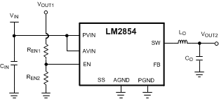 Figure 20. Simplified Schematic Showing EN Used to Cascade Power Supply Start-up
8.2.2.7 Output Voltage Setting
A divider resistor network from VOUT to the FB pin determines the desired output voltage as shown in Equation 11.

RFB1 is defined based on the voltage loop requirements and RFB2 is then selected for the desired output voltage. These resistors are normally selected as 0.5% or 1% tolerance.
8.2.2.8 Compensation Component Selection
The power stage transfer function of a voltage mode buck converter has a complex double pole related to the LC output filter and a left half plane zero due to the output capacitor ESR, denoted RESR. The locations of these singularities are given respectively in Equation 12.

where
- CO is the output capacitance value appropriately derated for applied voltage and operating temperature
- RL is the effective load resistance
- RDCR is the series damping resistance associated with the inductor and power switches
 Figure 21. LM2854 Compensation Scheme
The conventional compensation strategy employed with voltage mode control is to use two compensator zeros to offset the LC double pole, one compensator pole located to cancel the output capacitor ESR zero and one compensator pole located between one third and one half switching frequency for high frequency noise attenuation.
The LM2854 internal compensation components are designed to locate a pole at the origin and a pole at high frequency as mentioned above. Furthermore, a zero is located at 8.8 kHz or 17.6 kHz for the 500 kHz or 1 MHz options, respectively, to approximately cancel the likely location of one LC filter pole.
The three external compensation components, RFB1, RCOMP and CCOMP, are selected to position a zero at or below the LC pole location and a pole to cancel the ESR zero. The voltage loop crossover frequency, floop, is usually selected between one tenth to one fifth of the switching frequency, as shown in Equation 13.
A simple solution for the required external compensation capacitor, CCOMP, with type III voltage mode control can be expressed as in Equation 14.

where the constant α is nominally 0.038 or 0.075 for the 500 kHz or 1 MHz options, respectively. This assumes a compensator pole cancels the output capacitor ESR zero. Furthermore, since the modulator gain is proportional to VIN, the loop crossover frequency increases with VIN. Thus, it is recommended to design the loop at maximum expected VIN.
The upper feedback resistor, RFB1, is selected to provide adequate mid-band gain and to locate a zero at or below the LC pole frequency. The series resistor, RCOMP, is selected to locate a pole at the ESR zero frequency, as shown in Equation 15.

Note that the lower feedback resistor, RFB2, has no impact on the control loop from an AC standpoint since the FB pin is the input to an error amplifier and effectively at AC ground. Hence, the control loop can be designed irrespective of output voltage level. The only caveat here is the necessary derating of the output capacitance with applied voltage. Having chosen RFB1 as above, RFB2 is then selected for the desired output voltage.
Table 1 and Table 2 list inductor and ranges of capacitor values that work well with the LM2854, along with the associated compensation components to ensure stable operation. Values different than those listed may be used, but the compensation components may need to be recalculated to avoid degradation in phase margin. Note that the capacitance ranges specified refer to in-circuit values where the nominal capacitance value is adequately derated for applied voltage.
8.2.2.9 Filter Inductor and Output Capacitor Selection
In a buck regulator, selection of the filter inductor and capacitor will affect many key system parameters, including stability, transient response and efficiency The LM2854 can accommodate relatively wide ranges of output capacitor and filter inductor values in a typical application and still achieve excellent load current transient performance and low output voltage ripple.
The inductance is chosen such that the peak-to-peak inductor current ripple, ΔiL, is approximately 25 to 40% of IOUT as shown in Equation 16.

Note that the peak inductor current is the DC output current plus half the ripple current and reaches its highest level at lowest duty cycle (or highest VIN). It is recommended that the inductor should have a saturation current rating in excess of the current limit level.
When operating the LM2854 at input voltages above 5.2 V, the inductor should be sized to keep the minimum inductor current above –0.5 A. For most applications this should only occur at light loads or when the inductor is drastically undersized. To ensure the current never goes below –0.5 A for any application, the peak-to-peak ripple current (ΔiL) in the inductor should be less than 1 A. Keeping the minimum inductor current above –0.5 A limits the energy storage in the inductor and helps prevent the switch node voltage from exceeding the absolute maximum specification when the low side FET turns off.
Table 3 lists examples of off-the-shelf powdered iron and ferrite based inductors that are suitable for use with the LM2854. The output capacitor can be of ceramic or electrolytic chemistry. The chosen output capacitor requires sufficient DC voltage rating and RMS ripple current handling capability.
The output capacitor RMS current and peak-to-peak output ripple are given respectively as in Equation 17.

In general, 22 µF to 100 µF of ceramic output capacitance is sufficient for both LM2854 frequency options given the optimal high frequency characteristics and low ESR of ceramic dielectric. It is advisable to consult the manufacturer’s derating curves for capacitance voltage coefficient as the in-circuit capacitance may drop significantly with applied voltage.
Tantalum or organic polymer electrolytic capacitance may be suitable with the LM2854 500 kHz option, particularly in applications where substantial bulk capacitance per unit volume is required. However, the high loop bandwidth achievable with the LM2854 obviates the necessity for large bulk capacitance during transient loading conditions.
Table 4 lists some examples of commercially available capacitors that can be used with the LM2854.
Table 1. LM2854 500-kHz Compensation Component Values
| VIN (V) | LO (µH) | CO (µF) | ESR (mΩ) | RFB1 (kΩ) | CCOMP (pF) | RCOMP (kΩ) | ||
|---|---|---|---|---|---|---|---|---|
| MIN | MAX | MIN | MAX | |||||
| 5 | 1.5 | 40 | 100 | 2 | 10 | 150 | 47 | 1 |
| 1.5 | 100 | 200 | 1 | 5 | 150 | 100 | 1 | |
| 1.5 | 100 | 220 | 15 | 25 | 150 | 120 | 25 | |
| 2.2 | 40 | 100 | 2 | 10 | 150 | 68 | 1 | |
| 2.2 | 100 | 200 | 1 | 5 | 150 | 120 | 1 | |
| 2.2 | 100 | 220 | 15 | 25 | 120 | 120 | 15 | |
| 3.3 | 1.5 | 40 | 100 | 2 | 10 | 150 | 68 | 1 |
| 1.5 | 100 | 200 | 1 | 5 | 100 | 150 | 1 | |
| 1.5 | 100 | 220 | 15 | 25 | 100 | 150 | 15 | |
| 2.2 | 40 | 100 | 2 | 10 | 150 | 100 | 1 | |
| 2.2 | 100 | 200 | 1 | 5 | 100 | 220 | 1 | |
| 2.2 | 100 | 220 | 15 | 25 | 100 | 220 | 10 | |
Table 2. LM2854 1-MHz Compensation Component Values
| VIN (V) | LO (µH) | CO (µF) | ESR (mΩ) | RFB1 (kΩ) | CCOMP (pF) | RCOMP (kΩ) | ||
|---|---|---|---|---|---|---|---|---|
| MIN | MAX | MIN | MAX | |||||
| 5 | 0.68 | 20 | 60 | 2 | 10 | 120 | 33 | 1 |
| 0.68 | 60 | 150 | 1 | 5 | 75 | 100 | 1 | |
| 0.68 | 100 | 220 | 15 | 25 | 100 | 100 | 20 | |
| 1 | 20 | 60 | 2 | 10 | 100 | 56 | 1 | |
| 1 | 60 | 150 | 1 | 5 | 75 | 150 | 1 | |
| 1 | 100 | 220 | 15 | 25 | 75 | 150 | 15 | |
| 3.3 | 0.68 | 20 | 60 | 2 | 10 | 75 | 56 | 1 |
| 0.68 | 60 | 150 | 1 | 5 | 50 | 150 | 1 | |
| 0.68 | 100 | 220 | 15 | 25 | 50 | 150 | 12 | |
| 1 | 20 | 60 | 2 | 10 | 75 | 82 | 1 | |
| 1 | 60 | 150 | 1 | 5 | 50 | 220 | 1 | |
| 1 | 100 | 220 | 15 | 25 | 33 | 330 | 10 | |
Table 3. Recommended Filter Inductors
| INDUCTANCE (µH) | DCR (mΩ) | MANUFACTURER | MANUFACTURER P/N | CASE SIZE (mm) |
|---|---|---|---|---|
| 0.47 | 14.5 | Vishay Dale | IHLP1616BZERR47M11 | 4.06 × 4.45 × 2.00 |
| 1 | 24 | Vishay Dale | IHLP1616BZER1R0M11 | 4.06 × 4.45 × 2.00 |
| 0.47 | 8.4 | Vishay Dale | IHLP2525AHERR47M01 | 6.47 × 6.86 × 1.80 |
| 0.47 | 6 | Vishay Dale | IHLP2525BDERR47M01 | 6.47 × 6.86 × 2.40 |
| 0.68 | 8.7 | Vishay Dale | IHLP2525BDERR68M01 | 6.47 × 6.86 × 2.40 |
| 0.82 | 10.6 | Vishay Dale | IHLP2525BDERR82M01 | 6.47 × 6.86 × 2.40 |
| 1 | 13.1 | Vishay Dale | IHLP2525BDER1R0M01 | 6.47 × 6.86 × 2.40 |
| 1.5 | 18.5 | Vishay Dale | IHLP2525BDER1R5M01 | 6.47 × 6.86 × 2.40 |
| 2.2 | 15.7 | Vishay Dale | IHLP2525CZER2R2M11 | 6.47 × 6.86 × 3.00 |
| 0.47 | 3.5 | Sumida | CDMC6D28NP-R47M | 6.50 × 7.25 × 3.00 |
| 0.68 | 4.5 | Sumida | CDMC6D28NP-R68M | 6.50 × 7.25 × 3.00 |
| 1 | 17.3 | Sumida | CDMC6D28NP-1R0M | 6.50 × 7.25 × 3.00 |
| 1.5 | 10.4 | Sumida | CDMC6D28NP-1R5M | 6.50 × 7.25 × 3.00 |
| 2.2 | 16.1 | Sumida | CDMC6D28NP-2R2M | 6.50 × 7.25 × 3.00 |
| 0.56 | 10 | Coilcraft | DO1813H-561ML | 6.10 × 8.89 × 5.00 |
| 0.47 | 3.3 | Coilcraft | HA3619-471ALC | 7 × 7 × 3 |
| 0.68 | 4.8 | Coilcraft | HA3619-681ALC | 7 × 7 × 3 |
| 1 | 7.5 | Coilcraft | HA3619-102ALC | 7 × 7 × 3 |
| 1.2 | 9.4 | Coilcraft | HA3619-122ALC | 7 × 7 × 3 |
| 1.5 | 11.5 | Coilcraft | HA3619-152ALC | 7 × 7 × 3 |
| 1.8 | 16.5 | Coilcraft | HA3619-182ALC | 7 × 7 × 3 |
| 0.47 | 3.3 | TDK | SPM6530T-R47M170 | 7.1 × 6.5 × 3 |
| 0.68 | 4.9 | TDK | SPM6530T-R68M140 | 7.1 × 6.5 × 3 |
| 1 | 7.1 | TDK | SPM6530T-1R0M120 | 7.1 × 6.5 × 3 |
| 1.5 | 9.7 | TDK | SPM6530T-1R5M100 | 7.1 × 6.5 × 3 |
| 0.47 | 14 | Cyntec | PCMC042T-0R47MN | 4 × 4.5 × 2 |
| 1.0 | 9 | Cyntec | PCMC063T-1R0MN | 6.5 × 6.9 × 3 |
| 1.5 | 14 | Cyntec | PCMC063T-1R5MN | 6.5 × 6.9 × 3 |
Table 4. Recommended Filter Capacitors
| CAPACITANCE (µF) | VOLTAGE (V), ESR (mΩ) | CHEMISTRY | MANUFACTURER | MANUFACTURER P/N | CASE SIZE |
|---|---|---|---|---|---|
| 22 | 6.3, < 5 | Ceramic, X5R | TDK | C3216X5R0J226M | 1206 |
| 47 | 6.3, < 5 | Ceramic, X5R | TDK | C3216X5R0J476M | 1206 |
| 47 | 6.3, < 5 | Ceramic, X5R | TDK | C3225X5R0J476M | 1210 |
| 47 | 10, < 5 | Ceramic, X5R | TDK | C3225X5R1A476M | 1210 |
| 100 | 6.3, < 5 | Ceramic, X5R | TDK | C3225X5R0J107M | 1210 |
| 100 | 6.3, 50 | Tantalum | AVX | TPSD157M006#0050 | D, 7.5 × 4.3 × 2.9 mm |
| 100 | 6.3, 25 | Organic Polymer | Sanyo | 6TPE100MPB2 | B2, 3.5 × 2.8 × 1.9 mm |
| 150 | 6.3, 18 | Organic Polymer | Sanyo | 6TPE150MIC2 | C2, 6 × 3.2 × 1.8 mm |
| 330 | 6.3, 18 | Organic Polymer | Sanyo | 6TPE330MIL | D3L, 7.3 × 4.3 × 2.8 mm |
| 470 | 6.3, 23 | Niobium Oxide | AVX | NOME37M006#0023 | E, 7.3 × 4.3 × 4.1 mm |
8.2.3 Application Curves
Unless otherwise specified, the following conditions apply: VIN = PVIN = AVIN = EN = 5 V, CIN is 47-μF 10-V X5R ceramic capacitor, LO is from TDK SPM6530T family; TAMBIENT = 25°C.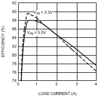 Figure 22. LM2854 1-MHz Efficiency vs IOUT VOUT = 0.8 V, LO = 0.47 µH, 3.3-mΩ DCR
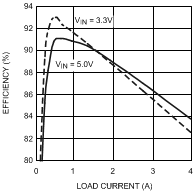 Figure 24. LM2854 1-MHz Efficiency vs IOUT VOUT = 1.2 V, LO = 0.68 µH, 4.9-mΩ DCR
 Figure 26. LM2854 1-MHz Efficiency vs IOUT VOUT = 1.8 V, LO = 1 µH, 7.1-mΩ DCR
 Figure 28. LM2854 500-kHz Efficiency vs IOUT VOUT = 2.5 V, LO = 2.2 µH, 16-mΩ DCR
 Figure 30. LM2854 500-kHz Efficiency vs IOUT VOUT = 3.3 V, LO = 1.5 µH, 9.7-mΩ DCR
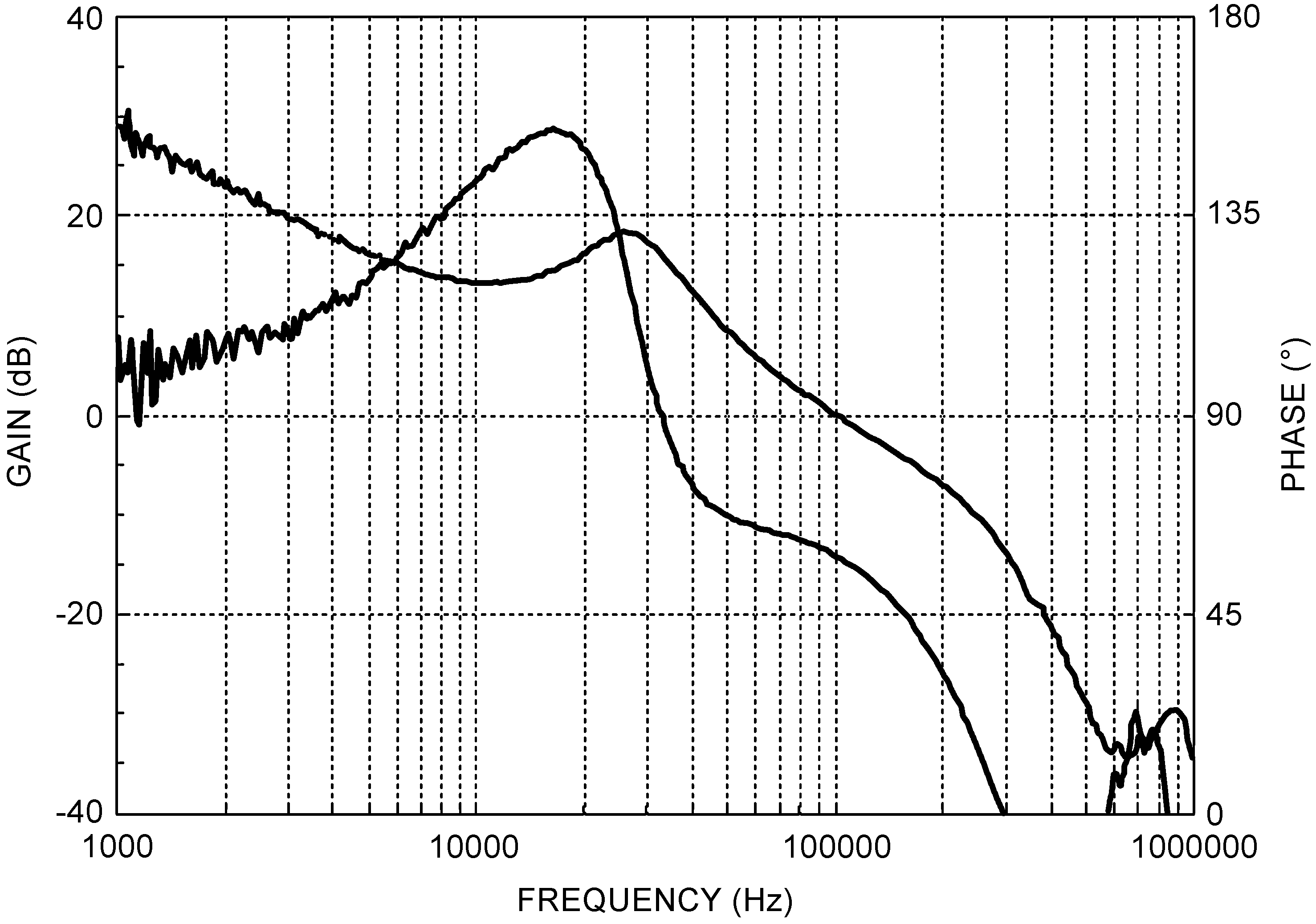 Figure 32. LM2854 1-MHz Bode Plot VIN = 3.3 V, VOUT = 1.8 V, IOUT = 4 A RFB1 = 150 kΩ, RCOMP = 1 kΩ, CCOMP = 100 pF, LOUT = 0.82 µH, COUT = 100-µF Ceramic
 Figure 34. LM2854 1-MHz Bode Plot VIN = 5 V, VOUT = 1.8 V, IOUT = 4 A RFB1 = 150 kΩ, RCOMP = 1 kΩ, CCOMP = 100 pF, LOUT = 0.82 µH, COUT = 100 µF
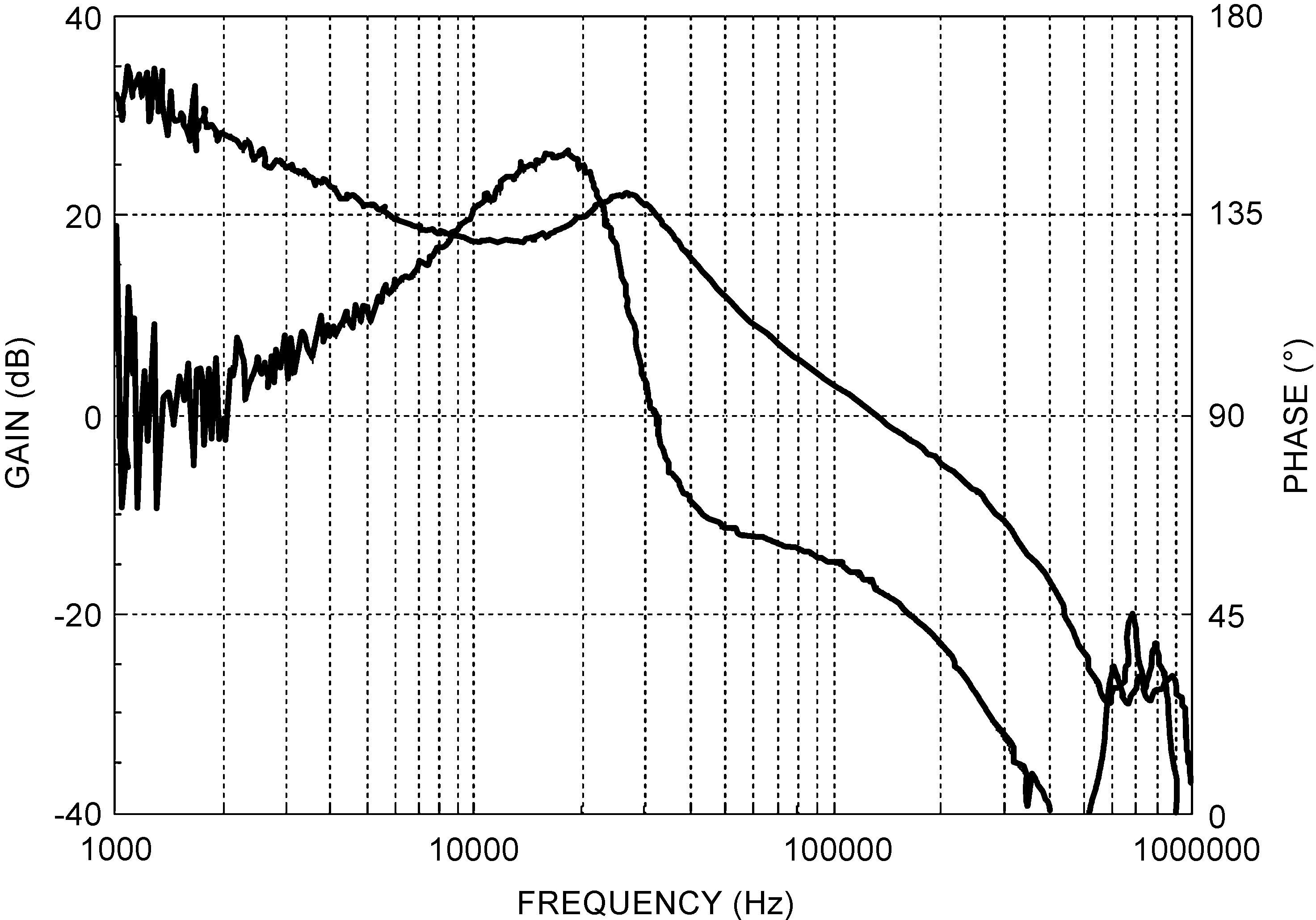 Figure 36. LM2854 1-MHz Bode Plot VIN = 5 V, VOUT = 3.3 V, IOUT = 4 A RFB1 = 150 kΩ, RCOMP = 1 kΩ, CCOMP = 68 pF, LOUT = 0.82 µH, COUT = 100-µF Ceramic
 Figure 38. LM2854 500-kHz Power On Characteristic
 VIN = 5 V, VOUT = 1.8 V, IOUT = 4 A, CSS = 220 pF
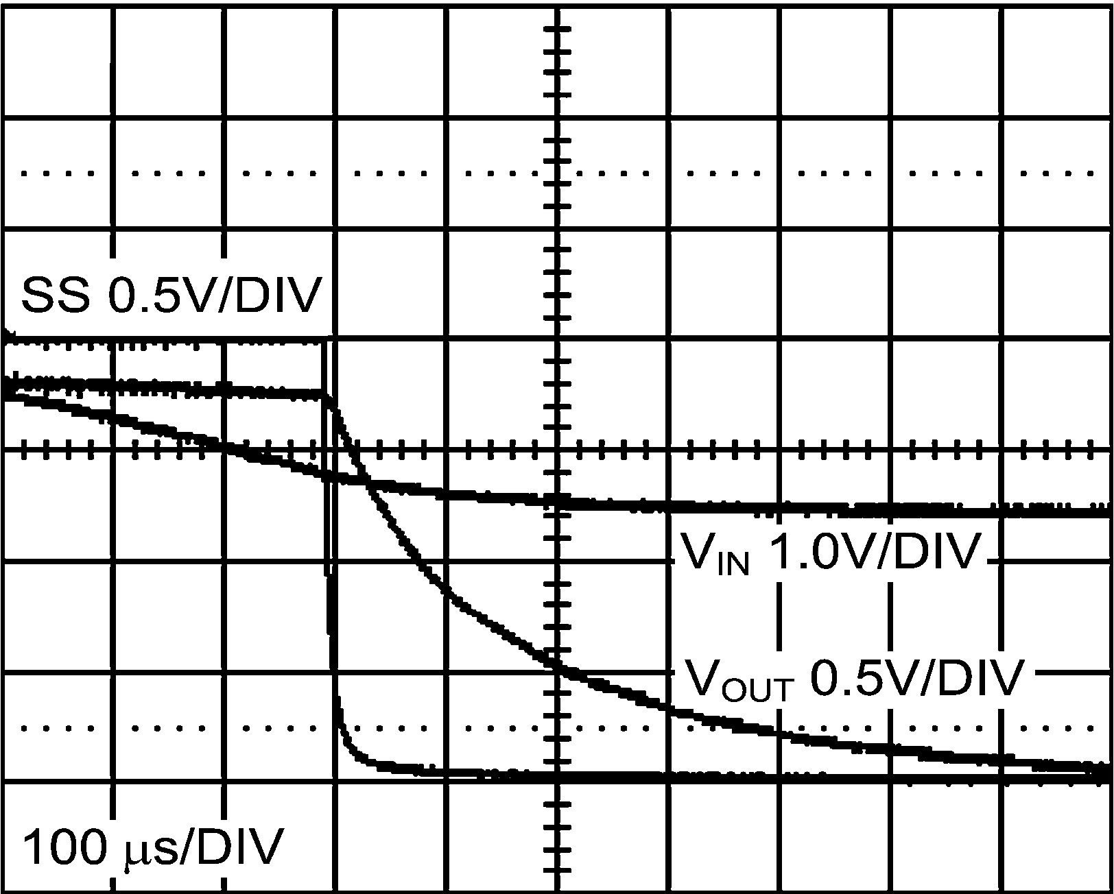 Figure 40. LM2854 500-kHz Power Off Characteristic
 VIN = 5 V, VOUT = 1.8 V, IOUT = 4 A, CSS = 220 pF
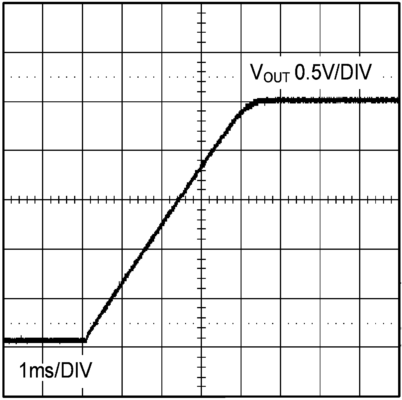 Figure 42. LM2854 500-kHz Start-up Waveform VOUT =
 2.5 V, IOUT = 0 A
 Figure 23. LM2854 1-MHz Efficiency vs IOUT VOUT = 2.5 V, LO = 1 µH, 7.1-mΩ DCR
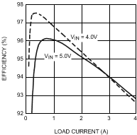 Figure 25. LM2854 1-MHz Efficiency vs IOUT VOUT = 3.3 V, LO = 1 µH, 7.1-mΩ DCR
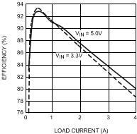 Figure 27. LM2854 500-kHz Efficiency vs IOUT VOUT = 0.8 V, LO = 1 µH, 7.1-mΩ DCR
 Figure 29. LM2854 500-kHz Efficiency vs IOUT VOUT = 1.2 V, LO = 1.5 µH, 9.7-mΩ DCR
 Figure 31. LM2854 500-kHz Efficiency vs IOUT VOUT = 1.8 V, LO = 1.5 µH, 9.7-mΩ DCR
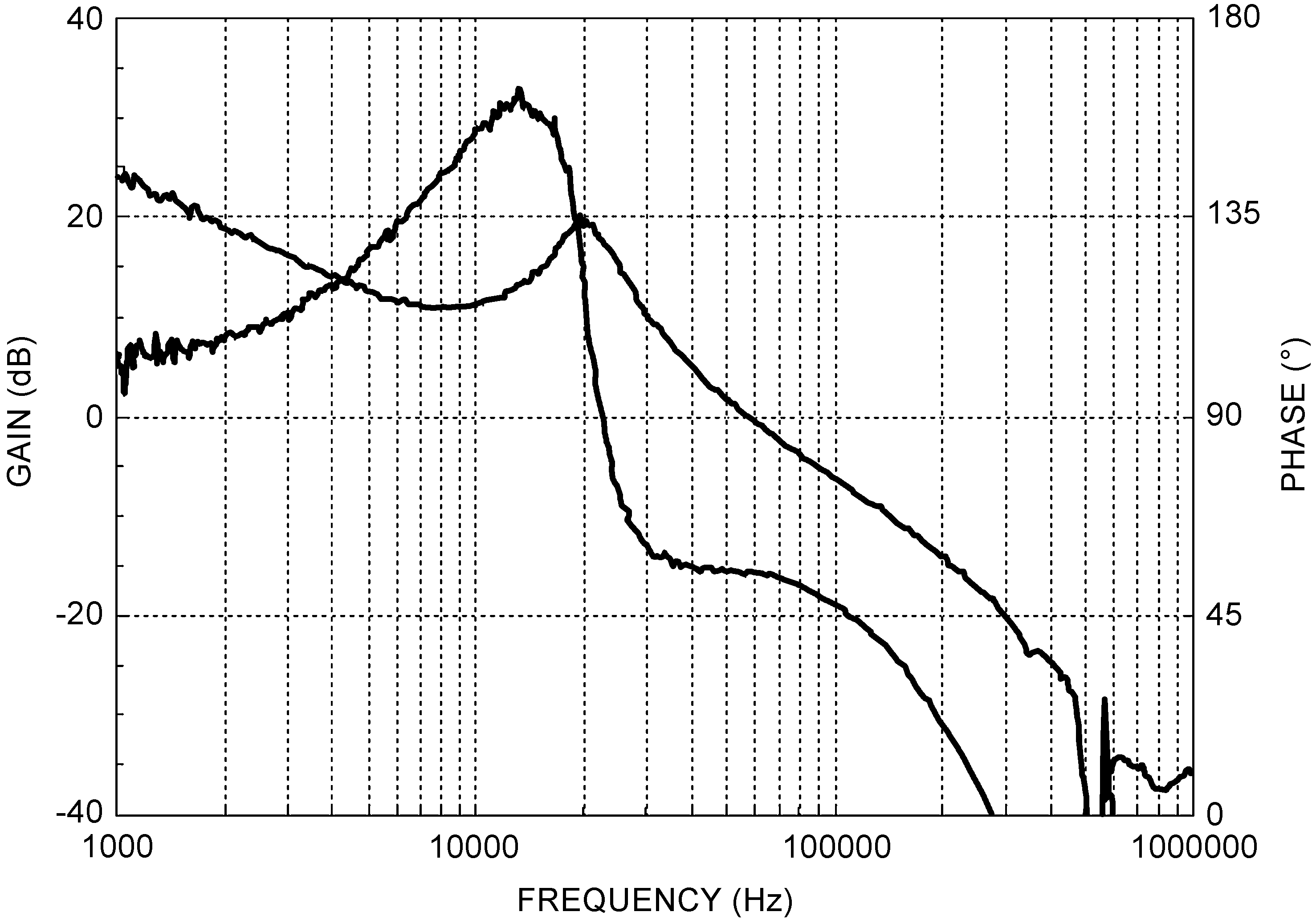 Figure 33. LM2854 500-kHz Bode Plot VIN = 3.3 V,
 VOUT = 1.8 V, IOUT = 4 A RFB1 = 250 kΩ, RCOMP = 1 kΩ, CCOMP = 47 pF, LOUT = 1.5 µH, COUT = 100-µF Ceramic
 Figure 35. LM2854 500-kHz Bode Plot VIN = 5 V,
 VOUT = 1.8 V, IOUT = 4 A RFB1 = 250 kΩ, RCOMP = 1 kΩ, CCOMP = 47 pF, LOUT = 1.5 µH, COUT = 100-µF Ceramic
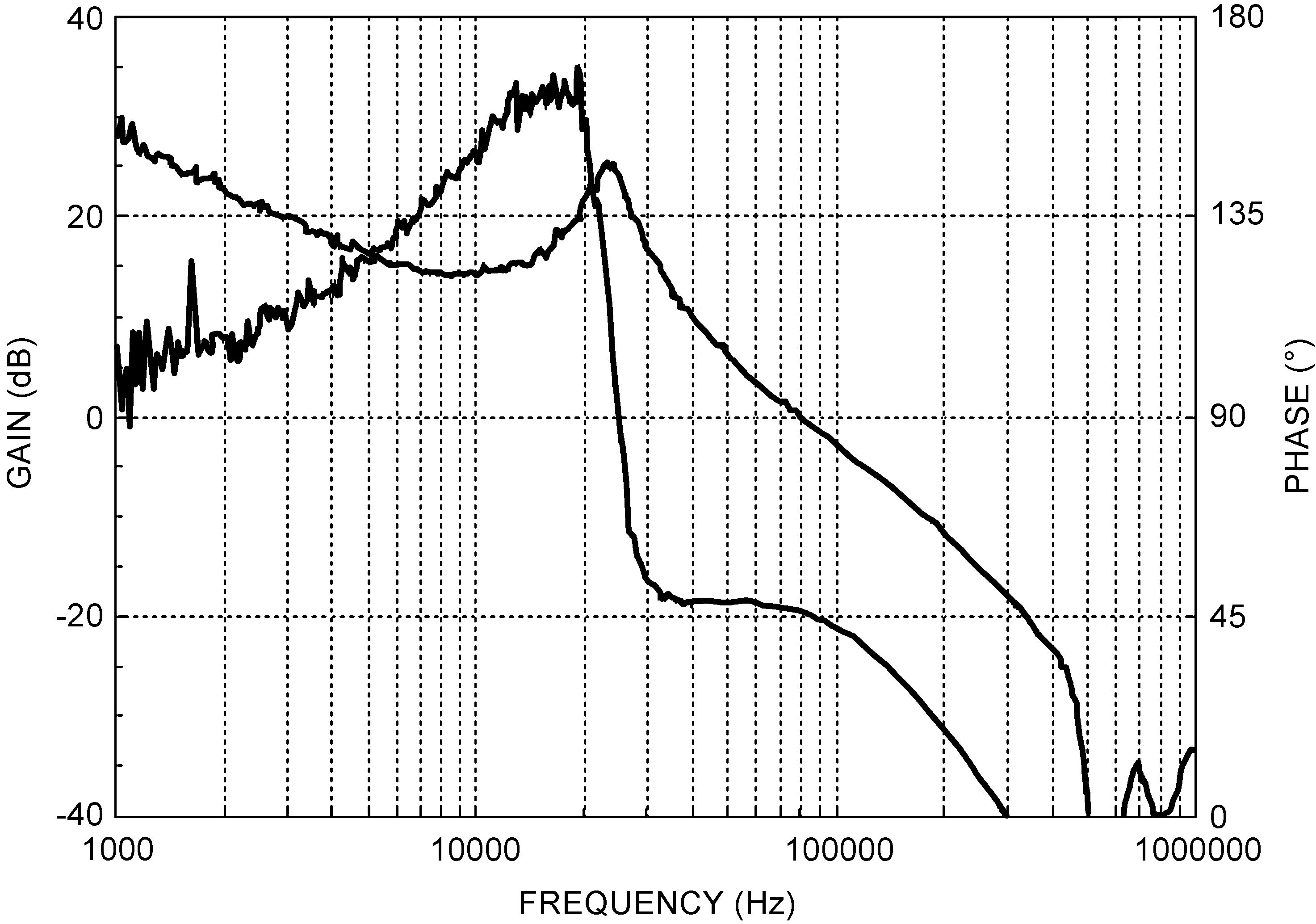 Figure 37. LM2854 500-kHz Bode Plot VIN = 5 V,
 VOUT = 3.3 V, IOUT = 4 A RFB1 = 250 kΩ, RCOMP = 1 kΩ, CCOMP = 33 pF, LOUT = 1.5 µH, COUT = 100-µF Ceramic
 Figure 39. LM2854 500-kHz Power On through Enable
 VIN = 5 V, VOUT = 1.8 V, IOUT = 4 A, CSS = 220 pF
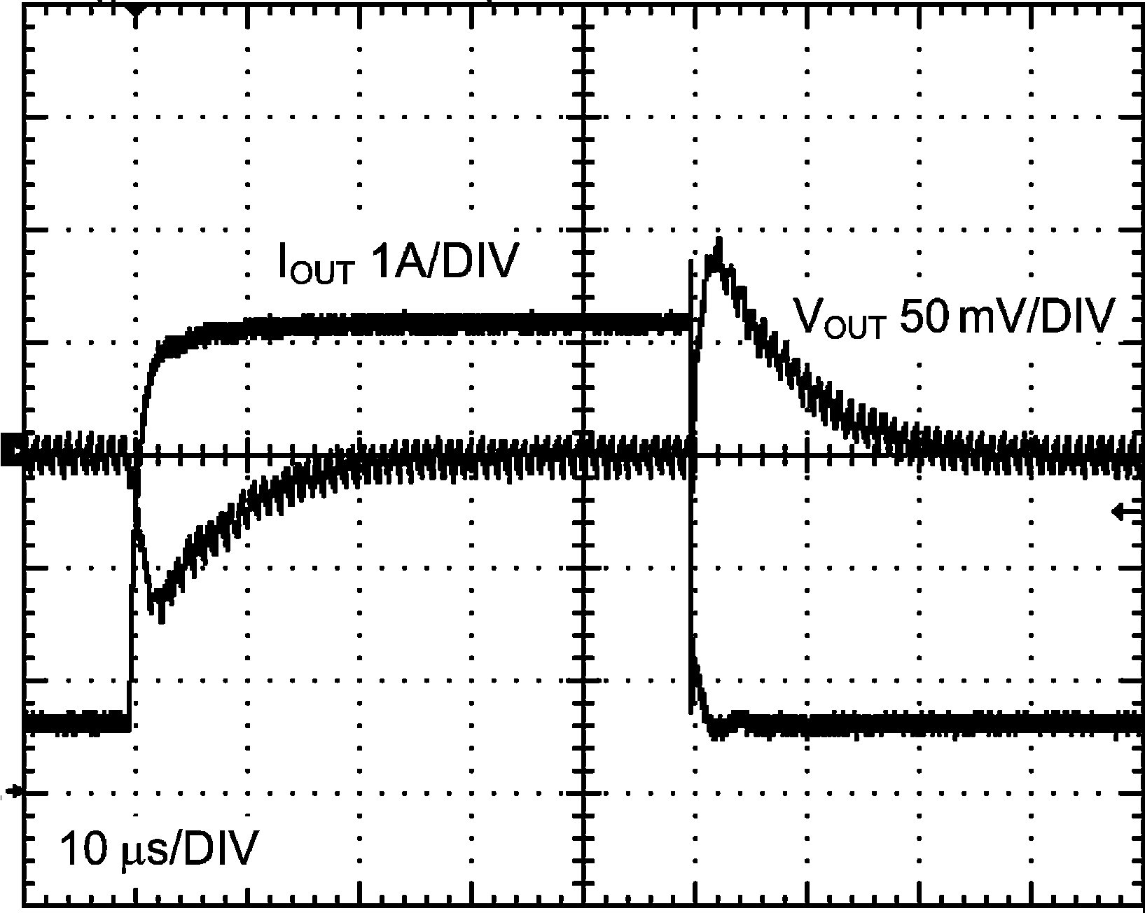 Figure 41. LM2854 1-MHz Load Transient Response
 VIN = 5 V, VOUT = 3.3 V, IOUT = 0.5-A to 4-A to 0.5-A step di/dt ≊ 4 A/µs, CO = 100-µF Ceramic
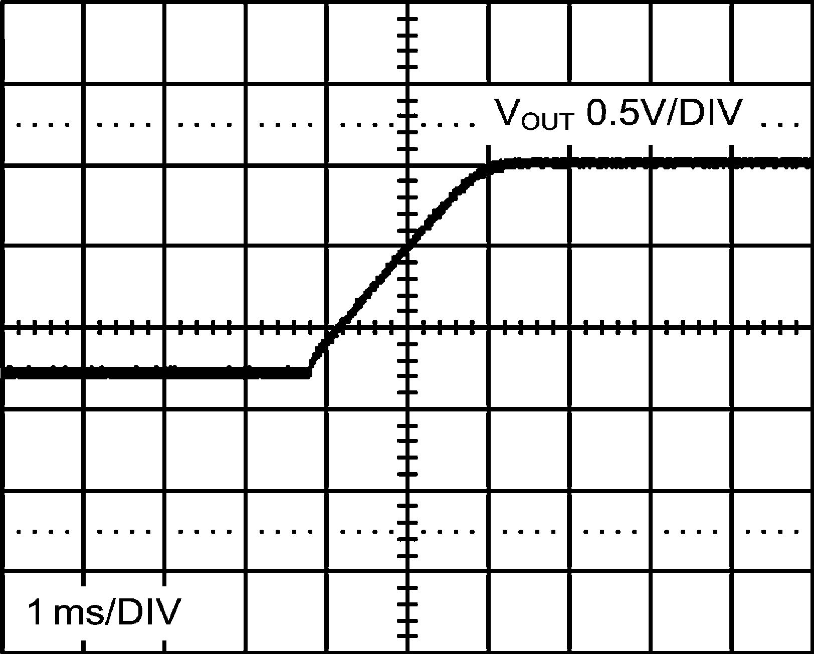 Figure 43. LM2854 500-kHz Pre-Biased Start-up Waveform (Oscilloscope Set at Infinite Persistence) VOUT = 2.5 V,
 IOUT = 0 A, VPRE-BIAS = 1.25 V
8.2.4 System Examples
This section provides several application solutions with an associated bill of materials, listed in Table 5 to Table 7. All bill of materials reference the schematic in Figure 44. The compensation for each solution was optimized to work over the full input range. Many applications have a fixed input voltage rail. It is possible to modify the compensation to obtain a faster transient response for a given input voltage operating point.
 Figure 44. LM2854 Application Circuit Schematic
Table 5. LM2854 500-kHz Bill of Materials, VIN = 5 V, VOUT = 3.3 V, IOUT(MAX) = 4 A, Optimized for Efficiency
| REF DES | DESCRIPTION | CASE SIZE | MANUFACTURER | MANUFACTURER P/N |
|---|---|---|---|---|
| U1 | Synchronous Buck Regulator | HTSSOP-16 | Texas Instruments | LM2854MHX-500 |
| CIN | 47 µF, X5R, 10 V | 1210 | TDK | C3225X5R1A476M |
| CO | 100 µF, X5R, 6.3 V | 1210 | TDK | C3225X5R0J107M |
| LO | 1.5 µH, 9.7 mΩ, 10 A | 7.1 × 6.5 × 3.0 mm | TDK | SPM6530T-1R5M100 |
| RFB1 | 249 kΩ | 0603 | Vishay Dale | CRCW06032493F-e3 |
| RFB2 | 80.6 kΩ | 0603 | Vishay Dale | CRCW060328062F-e3 |
| RCOMP | 1 kΩ | 0603 | Vishay Dale | CRCW06031001F-e3 |
| RF | 1 Ω | 0603 | Vishay Dale | CRCW06031R0F-e3 |
| CCOMP | 33 pF, ±5%, C0G, 50 V | 0603 | TDK | C1608C0G1H330J |
| CSS | 10 nF, ±10%, X7R, 16 V | 0603 | Murata | GRM188R71C103KA01 |
| CF | 1.0 µF, ±10%, X7R, 10 V | 0603 | Murata | GRM188R71A105KA61 |
Table 6. LM2854 1-MHz Bill of Materials, VIN = 3.3 V to 5 V, VOUT = 2.5 V, IOUT (MAX) = 4 A, Optimized for Electrolytic Input and Output Capacitance
| REF DES | DESCRIPTION | CASE SIZE | MANUFACTURER | MANUFACTURER P/N |
|---|---|---|---|---|
| U1 | Synchronous Buck Regulator | HTSSOP-16 | Texas Instruments | LM2854MHX-1000 |
| CIN | 150 µF, 6.3 V, 18 mΩ | C2, 6 × 3.2 × 1.8 mm | Sanyo | 6TPE150MIC2 |
| CO | 330 µF, 6.3 V, 18 mΩ | D3L, 7.3 × 4.3 × 2.8 mm | Sanyo | 6TPE330MIL |
| LO | 2.2 µH, 16 mΩ, 7 A | 6.47 × 6.86 × 3 mm | Vishay Dale | IHLP2525CZER2R2M11 |
| RFB1 | 100 kΩ | 0603 | Vishay Dale | CRCW06031003F-e3 |
| RFB2 | 47.5 kΩ | 0603 | Vishay Dale | CRCW060324752F-e3 |
| RCOMP | 15 kΩ | 0603 | Vishay Dale | CRCW06031502F-e3 |
| RF | 1 Ω | 0603 | Vishay Dale | CRCW06031R0F-e3 |
| CCOMP | 330 pF, ±5%, C0G, 50 V | 0603 | TDK | C1608C0G1H331J |
| CSS | 10 nF, ±10%, X7R, 16 V | 0603 | Murata | GRM188R71C103KA01 |
| CF | 1 µF,±10%, X7R, 10 V | 0603 | Murata | GRM188R71A105KA61 |
Table 7. LM2854 1-MHz Bill of Materials, VIN = 3.3 V, VOUT = 0.8 V, IOUT (MAX) = 4 A, Optimized for Solution Size and Transient Response
| REF DES | DESCRIPTION | CASE SIZE | MANUFACTURER | MANUFACTURER P/N |
|---|---|---|---|---|
| U1 | Synchronous Buck Regulator | HTSSOP-16 | Texas Instruments | LM2854MHX-1000 |
| CIN | 47 µF, X5R, 6.3 V | 1206 | TDK | C3216X5R0J476M |
| CO | 47 µF, X5R, 6.3 V | 1206 | TDK | C3216X5R0J476M |
| LO | 0.47 µH, 14.5 mΩ, 7 A | 4.06 × 4.45 × 2.00 mm | Vishay Dale | IHLP1616BZER0R47M11 |
| RFB1 | 110 kΩ | 0402 | Vishay Dale | CRCW04021103F-e3 |
| RCOMP | 1 kΩ | 0402 | Vishay Dale | CRCW04021001F-e3 |
| RF | 1 Ω | 0402 | Vishay Dale | CRCW04021R0F-e3 |
| CCOMP | 27 pF, ±5%, C0G, 50 V | 0402 | Murata | GRM1555C1H270JZ01 |
| CSS | 10 nF, ±10%, X7R, 16 V | 0402 | Murata | GRM155R71C103KA01 |
| CF | 1 µF, ±10%, X7R, 10 V | 0402 | Murata | GRM155R61A105KE15 |