SNVS560E March 2008 – October 2017 LM2854
PRODUCTION DATA.
- 1 Features
- 2 Applications
- 3 Description
- 4 Revision History
- 5 Pin Configuration and Functions
- 6 Specifications
- 7 Detailed Description
-
8 Application and Implementation
- 8.1 Application Information
- 8.2
Typical Application
- 8.2.1 Design Requirements
- 8.2.2
Detailed Design Procedure
- 8.2.2.1 Input Filter Capacitor
- 8.2.2.2 AVIN Filtering Components
- 8.2.2.3 Soft-Start Capacitor
- 8.2.2.4 Tracking - Equal Soft-Start Time
- 8.2.2.5 Tracking - Equal Slew Rates
- 8.2.2.6 Enable and UVLO
- 8.2.2.7 Output Voltage Setting
- 8.2.2.8 Compensation Component Selection
- 8.2.2.9 Filter Inductor and Output Capacitor Selection
- 8.2.3 Application Curves
- 8.2.4 System Examples
- 9 Power Supply Recommendations
- 10Layout
- 11Device and Documentation Support
- 12Mechanical, Packaging, and Orderable Information
Package Options
Mechanical Data (Package|Pins)
- PWP|16
Thermal pad, mechanical data (Package|Pins)
- PWP|16
Orderable Information
6 Specifications
6.1 Absolute Maximum Ratings
over operating free-air temperature range (unless otherwise noted) (1)(2)| MIN | MAX | UNIT | ||
|---|---|---|---|---|
| PVIN, AVIN, SW, EN, FB, SS to GND(4) | –0.3 | 6 | V | |
| Power Dissipation | Internally Limited | |||
| Junction Temperature | 150 | °C | ||
| Storage Temperature | −65 | 150 | °C | |
(1) Stresses beyond those listed under Absolute Maximum Ratings may cause permanent damage to the device. These are stress ratings only, which do not imply functional operation of the device at these or any other conditions beyond those indicated under Recommended Operating Conditions. Exposure to absolute-maximum-rated conditions for extended periods may affect device reliability.
(2) If Military/Aerospace specified devices are required, please contact the Texas Instruments Sales Office/ Distributors for availability and specifications.
6.2 ESD Ratings
| VALUE | UNIT | |||
|---|---|---|---|---|
| V(ESD) | Electrostatic discharge | Human-body model (HBM), per ANSI/ESDA/JEDEC JS-001(1)(2) | ±2000 | V |
(1) JEDEC document JEP155 states that 500-V HBM allows safe manufacturing with a standard ESD control process.
(2) The human body model is a 100-pF capacitor discharged through a 1.5-kΩ resistor into each pin. Test method is per JESD22-AI14.
6.3 Recommended Operating Conditions
| MIN | MAX | UNIT | |
|---|---|---|---|
| PVIN to GND(4) | 2.95 | 5.5 | V |
| AVIN to GND(4) | 2.95 | 5.5 | V |
| Junction Temperature | −40 | 125 | °C |
6.4 Thermal Information
| THERMAL METRIC(1) | LM2854 | UNIT | |
|---|---|---|---|
| PWP (HTSSOP) | |||
| 16 PINS | |||
| RθJA | Junction-to-ambient thermal resistance | 38.4 | °C/W |
| RθJC(top) | Junction-to-case (top) thermal resistance | 27.6 | °C/W |
| RθJB | Junction-to-board thermal resistance | 17.1 | °C/W |
| ψJT | Junction-to-top characterization parameter | 1.5 | °C/W |
| ψJB | Junction-to-board characterization parameter | 16.9 | °C/W |
| RθJC(bot) | Junction-to-case (bottom) thermal resistance | 1.3 | °C/W |
(1) For more information about traditional and new thermal metrics, see the Semiconductor and IC Package Thermal Metrics application report, Semiconductor and IC Package Thermal Metrics.
6.5 Electrical Characteristics
All Typical specifications are for TJ = 25°C only; all Maximum and Minimum limits apply over the operating junction temperature range TJ range of –40°C to 125°C. Minimum and maximum limits are ensured through test, design, or statistical correlation. Typical values represent the most likely parametric norm at TJ = 25°C, and are provided for reference purposes only. AVIN = PVIN = EN = 5 V, unless otherwise indicated in the Test Conditions column.| PARAMETER | TEST CONDITIONS | MIN(1) | TYP(2) | MAX(1) | UNIT | |
|---|---|---|---|---|---|---|
| SYSTEM PARAMETERS | ||||||
| VREF | Reference Voltage(3) | Measured at the FB pin | 0.790 | 0.8 | 0.808 | V |
| ΔVREF/ΔAVIN | Line Regulation(3) | ΔAVIN = 2.95 V to 5.50 V | 0.04% | 0.6% | ||
| ΔVREF/ΔIO | Load Regulation | Normal operation | 0.25 | mV/A | ||
| VON | UVLO Threshold (AVIN) | Rising | 2.6 | 2.95 | V | |
| Falling hysteresis | 25 | 170 | 375 | mV | ||
| RDS(ON)-P | PFET On Resistance | ISW = 4 A | 35 | 65 | mΩ | |
| RDS(ON)-N | NFET On Resistance | ISW = 4 A | 34 | 65 | mΩ | |
| ISS | Soft-Start Current | 2 | µA | |||
| ICL | Peak Current Limit Threshold | 4.5 | 6 | 6.7 | A | |
| IQ | Operating Current | Non-switching | 1.7 | 3 | mA | |
| ISD | Shut Down Quiescent Current | EN = 0 V | 230 | 500 | µA | |
| PWM SECTION | ||||||
| fSW | Switching Frequency | 1-MHz option | 800 | 1050 | 1160 | kHz |
| 500-kHz option | 400 | 525 | 580 | kHz | ||
| Drange | PWM Duty Cycle Range | 0% | 100% | |||
| ENABLE CONTROL | ||||||
| VIH | EN Pin Rising Threshold | 0.8 | 1.23 | 1.65 | V | |
| VEN(HYS) | EN Pin Hysteresis | 150 | mV | |||
| THERMAL CONTROL | ||||||
| TSD | TJ for Thermal Shutdown | 165 | °C | |||
| TSD-HYS | Hysteresis for Thermal Shutdown | 10 | °C | |||
(1) Min and Max limits are 100% production tested at 25°C. Limits over the operating temperature range are ensured through correlation using Statistical Quality Control (SQC) methods. Limits are used to calculate Average Outgoing Quality Level (AOQL).
(2) Typical numbers are at 25°C and represent the most likely parametric norm.
(3) VREF measured in a non-switching, closed-loop configuration.
(4) PGND and AGND are electrically connected together on the PC board and the resultant net is termed GND.
6.6 Typical Characteristics
Unless otherwise specified, the following conditions apply: VIN = PVIN = AVIN = EN = 5, TJ = 25°C. Figure 1. Feedback Voltage vs Temperature
 Figure 3. Soft Start Current vs Temperature
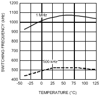
 Figure 5. Switching Frequency vs Temperature
 Figure 7. NMOS RDS(ON) vs Temperature
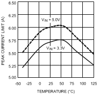
 Figure 9. Peak Current Limit vs Temperature
 Figure 11. IQ (disabled) vs VIN and Temperature, EN = 0 V
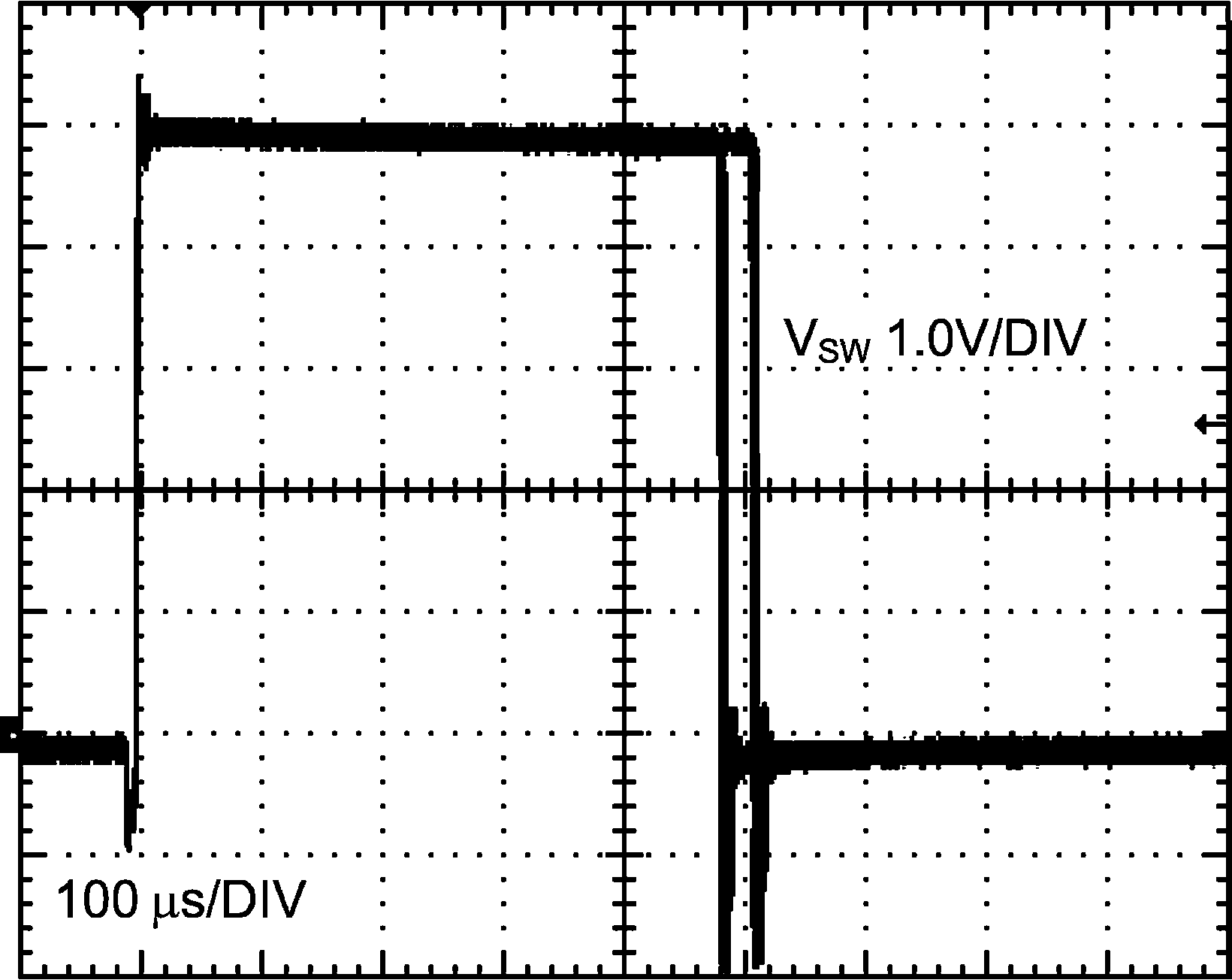
 Figure 13. LM2854 500-kHz Switch Node Voltage (oscilloscope set at infinite persistence) VIN = 5 V, VOUT = 2.5 V, IOUT = 4 A
 Figure 2. UVLO Threshold vs Temperature
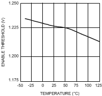
 Figure 4. Enable Threshold vs Temperature
 Figure 6. PMOS RDS(ON) vs Temperature
 Figure 8. IQ (operating) vs VIN and Temperature
 Figure 10. Feedback Voltage vs VIN
 Figure 12. Switching Frequency vs VIN