SLCS142G December 2003 – March 2023 LM2901-Q1 , LM2901AV-Q1 , LM2901B-Q1 , LM2901V-Q1
PRODMIX
- 1 Features
- 2 Applications
- 3 Description
- 4 Revision History
- 5 Pin Configuration and Functions
-
6 Specifications
- 6.1 Absolute Maximum Ratings for LM2901B-Q1
- 6.2 Absolute Maximum Ratings for LM2901x-Q1
- 6.3 ESD Ratings for LM2901B-Q1
- 6.4 ESD Ratings for LM2901x-Q1
- 6.5 Recommended Operating Conditions for LM2901B-Q1
- 6.6 Recommended Operating Conditions for LM2901x-Q1
- 6.7 Thermal Information for LM2901B-Q1
- 6.8 Thermal Information for LM2901x-Q1
- 6.9 Electrical Characteristics for LM2901B-Q1
- 6.10 Switching Characteristics for LM2901B-Q1
- 6.11 Electrical Characteristics for LM2901x-Q1
- 6.12 Switching Characteristics for LM2901x-Q1
- 6.13 Typical Characteristics: LM2901B-Q1
- 6.14 Typical Characteristics: LM2901x-Q1
- 7 Detailed Description
- 8 Application and Implementation
- 9 Power Supply Recommendations
- 10Layout
- 11Device and Documentation Support
- 12Mechanical, Packaging, and Orderable Information
Package Options
Refer to the PDF data sheet for device specific package drawings
Mechanical Data (Package|Pins)
- D|14
- PW|14
- RTE|16
Thermal pad, mechanical data (Package|Pins)
- RTE|16
Orderable Information
8.2.3 Application Curves
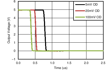
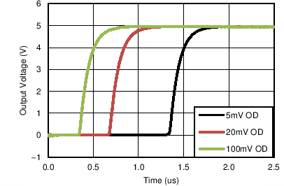
The following curves were generated with 5 V on VCC and VLOGIC, RPULLUP = 5.1 kΩ, and 50-pF scope probe.
 Figure 8-2 Response Time for Various Overdrives Negative Transition
 Figure 8-3 Response Time for Various Overdrives Positive Transition