SNOSBT3J January 2000 – March 2022 LM158-N , LM258-N , LM2904-N , LM358-N
PRODUCTION DATA
- 1 Features
- 2 Applications
- 3 Description
- 4 Revision History
- 5 Pin Configuration and Functions
- 6 Specifications
- 7 Detailed Description
- 8 Application and Implementation
- 9 Power Supply Recommendations
- 10Layout
- 11Device and Documentation Support
- 12Mechanical, Packaging, and Orderable Information
Package Options
Mechanical Data (Package|Pins)
Thermal pad, mechanical data (Package|Pins)
Orderable Information
7.4 Device Functional Modes
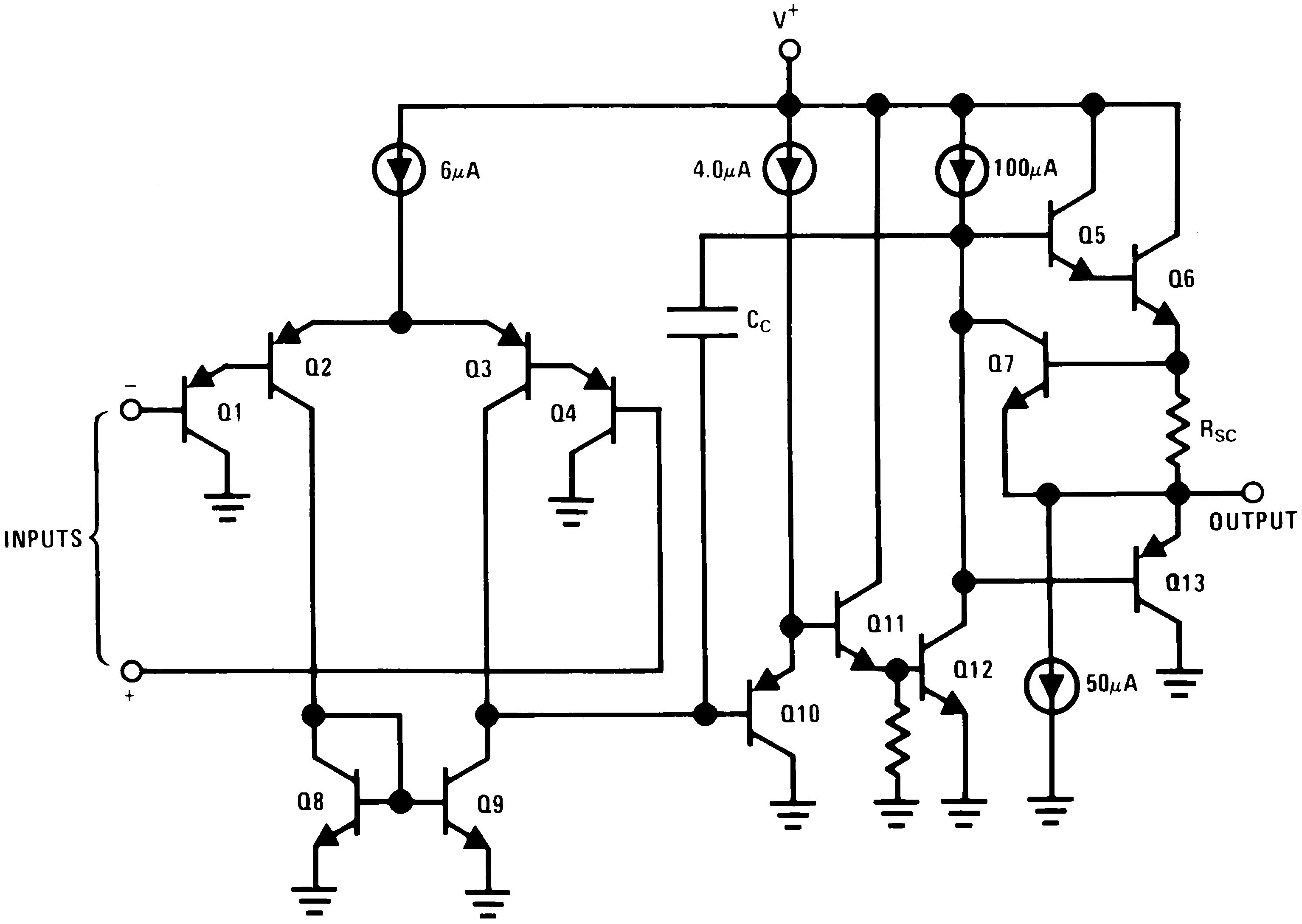
 Figure 7-2 Schematic Diagram
The circuits presented in the Typical Single-Supply Applications emphasize operation on only a single power supply voltage. If complementary power supplies are available, all of the standard op-amp circuits can be used. In general, introducing a pseudo-ground (a bias voltage reference of V+/2) will allow operation above and below this value in single power supply systems. Many application circuits are shown which take advantage of the wide input common-mode voltage range which includes ground. In most cases, input biasing is not required and input voltages which range to ground can easily be accommodated.