SBOS987B August 2020 – October 2021 LM2902LV-Q1 , LM2904LV-Q1
PRODUCTION DATA
- 1 Features
- 2 Applications
- 3 Description
- 4 Revision History
- 5 Pin Configuration and Functions
- 6 Specifications
- 7 Detailed Description
- 8 Application and Implementation
- 9 Power Supply Recommendations
- 10Layout
- 11Device and Documentation Support
- 12Mechanical, Packaging, and Orderable Information
Package Options
Mechanical Data (Package|Pins)
Thermal pad, mechanical data (Package|Pins)
Orderable Information
3 Description
The LM290xLV-Q1 family includes the dual LM2904LV-Q1 and quad LM2902LV-Q1 operational amplifiers, or op amps. The devices can operate in a supply range of 2.7 V to 5.5 V.
These op amps serves as supply an alternatives to the LM2904-Q1 and LM2902-Q1 in low-voltage applications that are sensitive to cost. The LM290xLV-Q1 devices provide better performance than the LM290x-Q1 devices at low voltage and have lower power consumption. The op amps are stable at unity gain, and do not have phase reversal in overdrive conditions. The design for ESD gives the LM290xLV-Q1 family an HBM specification of 2 kV.
The LM290xLV-Q1 family is available in packages that match industry standards. The available packages include SOIC, VSSOP, and TSSOP packages.
| PART NUMBER (1) | PACKAGE | BODY SIZE (NOM) |
|---|---|---|
| LM2902LV-Q1 | SOIC (14) | 8.65 mm × 3.91 mm |
| TSSOP (14) | 4.40 mm × 5.00 mm | |
| SOT23 (14) | 4.20 mm × 1.90 mm | |
| LM2904LV-Q1 | SOIC (8) | 3.91 mm × 4.90 mm |
| VSSOP (8) | 3.00 mm × 3.00 mm |
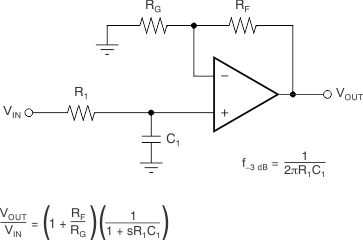
 Single-Pole, Low-Pass Filter