SNAS555D June 2000 – December 2016 LM2907-N , LM2917-N
PRODUCTION DATA.
- 1 Features
- 2 Applications
- 3 Description
- 4 Revision History
- 5 Description (continued)
- 6 Pin Configuration and Functions
- 7 Specifications
- 8 Parameter Measurement Information
- 9 Detailed Description
-
10Application and Implementation
- 10.1 Application Information
- 10.2
Typical Applications
- 10.2.1 Minimum Component Tachometer
- 10.2.2
Other Application Circuits
- 10.2.2.1 Variable Reluctance Magnetic Pickup Buffer Circuits
- 10.2.2.2 Finger Touch or Contact Switch
- 10.2.2.3 Over-Speed Latch
- 10.2.2.4 Frequency Switch Applications
- 10.2.2.5 Anti-Skid Circuits
- 10.2.2.6 Changing the Output Voltage for an Input Frequency of Zero
- 10.2.2.7 Changing Tachometer Gain Curve or Clamping the Minimum Output Voltage
- 11Power Supply Recommendations
- 12Layout
- 13Device and Documentation Support
- 14Mechanical, Packaging, and Orderable Information
Package Options
Mechanical Data (Package|Pins)
Thermal pad, mechanical data (Package|Pins)
Orderable Information
7 Specifications
7.1 Absolute Maximum Ratings
over operating free-air temperature range (unless otherwise noted)(1)(2)| MIN | MAX | UNIT | |||
|---|---|---|---|---|---|
| Supply voltage | 28 | V | |||
| Supply current (Zener options) | 25 | mA | |||
| Collector voltage | 28 | V | |||
| Differential input voltage | Tachometer, op amp, and comparator | 28 | V | ||
| Input voltage | Tachometer | LM2907 (8), LM2917 (8) | –28 | 28 | V |
| LM2907 (14), LM2917 (14) | 0 | 28 | |||
| Op amp and comparator | 0 | 28 | |||
| Power dissipation | LM29x7 (8) | 1200 | mW | ||
| LM29x7 (14) | 1580 | ||||
| Soldering information | PDIP package | Soldering (10 s) | 260 | °C | |
| SOIC package | Vapor phase (60 s) | 215 | |||
| Infrared (15 s) | 220 | ||||
| Operating temperature, TJ | –40 | 85 | °C | ||
| Storage temperature, Tstg | –65 | 150 | °C | ||
(1) Stresses beyond those listed under Absolute Maximum Ratings may cause permanent damage to the device. These are stress ratings only, which do not imply functional operation of the device at these or any other conditions beyond those indicated under Recommended Operating Conditions. Exposure to absolute-maximum-rated conditions for extended periods may affect device reliability.
(2) If Military/Aerospace specified devices are required, please contact the Texas Instruments Sales Office/Distributors for availability and specifications.
7.2 ESD Ratings
| VALUE | UNIT | |||
|---|---|---|---|---|
| V(ESD) | Electrostatic discharge | Human-body model (HBM), per ANSI/ESDA/JESD22-A114(1) | ±1000 | V |
| Charged-device model (CDM), per JEDEC specification JESD22-C101(2) | ±250 | |||
(1) JEDEC document JEP155 states that 500-V HBM allows safe manufacturing with a standard ESD control process.
(2) JEDEC document JEP157 states that 250-V CDM allows safe manufacturing with a standard ESD control process.
7.3 Recommended Operating Conditions
over operating free-air temperature range (unless otherwise noted)| MIN | NOM | MAX | UNIT | ||
|---|---|---|---|---|---|
| Input voltage | LM2907 (8), LM2917 (8) | –28 | 28 | V | |
| LM2907 (14), LM2917 (14) | 0 | 28 | V | ||
| Output sink current | 50 | mA | |||
7.4 Thermal Information
| THERMAL METRIC(1) | LM2907, LM2917 | UNIT | ||||
|---|---|---|---|---|---|---|
| P (PDIP) | D (SOIC) | NFF (PDIP) | D (SOIC) | |||
| 8 PINS | 8 PINS | 14 PINS | 14 PINS | |||
| RθJA | Junction-to-ambient thermal resistance | 77.6 | 110 | 69.1 | 83.7 | °C/W |
| RθJC(top) | Junction-to-case (top) thermal resistance | 80.5 | 53.9 | 64.8 | 42.1 | °C/W |
| RθJB | Junction-to-board thermal resistance | 54.8 | 50.4 | 49.1 | 38 | °C/W |
| ψJT | Junction-to-top characterization parameter | 37.6 | 9.1 | 35.1 | 7.7 | °C/W |
| ψJB | Junction-to-board characterization parameter | 54.8 | 49.9 | 49 | 37.7 | °C/W |
| RθJC(bot) | Junction-to-case (bottom) thermal resistance | — | — | — | — | °C/W |
(1) For more information about traditional and new thermal metrics, see the Semiconductor and IC Package Thermal Metrics application report.
7.5 Electrical Characteristics
VCC = 12 VDC, TA = 25°C, see test circuit| PARAMETER | TEST CONDITIONS | MIN | TYP | MAX | UNIT | |
|---|---|---|---|---|---|---|
| TACHOMETER | ||||||
| Input thresholds | VIN = 250 mVp-p at 1 kHz(1) | ±10 | ±25 | ±40 | mV | |
| Hysteresis | VIN = 250 mVp-p at 1 kHz(1) | 30 | mV | |||
| LM29x7 offset voltage | VIN = 250 mVp-p at 1 kHz(1) | 3.5 | 10 | mV | ||
| VIN = 250 mVp-p at 1 kHz (8-pin LM29x7)(1) | 5 | 15 | ||||
| Input bias current | VIN = ±50 mVDC | 0.1 | 1 | μA | ||
| VOH | High level output voltage | For CP1, VIN = 125 mVDC(2) | 8.3 | V | ||
| VOL | Low level output voltage | For CP1, VIN = –125 mVDC(2) | 2.3 | V | ||
| I2, I3 | Output current | V2 = V3 = 6 V(3) | 140 | 180 | 240 | μA |
| I3 | Leakage current | I2 = 0, V3 = 0 | 0.1 | μA | ||
| K | Gain constant | See(2) | 0.9 | 1 | 1.1 | |
| Linearity | fIN = 1 kHz, 5 kHz, or 10 kHz(4) | –1% | 0.3% | 1% | ||
| OP AMP AND COMPARATOR | ||||||
| VOS | Input offset voltage | VIN = 6 V | 3 | 10 | mV | |
| IBIAS | Bias current | VIN = 6 V | 50 | 500 | nA | |
| Input common-mode voltage | 0 | VCC–1.5 | V | |||
| Voltage gain | 200 | V/mV | ||||
| Output sink current | VC = 1 | 40 | 50 | mA | ||
| Output source current | VE = VCC –2 | 10 | mA | |||
| Saturation voltage | ISINK = 5 mA | 0.1 | 0.5 | V | ||
| ISINK = 20 mA | 1 | V | ||||
| ISINK = 50 mA | 1 | 1.5 | V | |||
| ZENER REGULATOR | ||||||
| Regulator voltage | RDROP = 470 Ω | 7.56 | V | |||
| Series resistance | 10.5 | 15 | Ω | |||
| Temperature stability | 1 | mV/°C | ||||
| Total supply current | 3.8 | 6 | mA | |||
(1) Hysteresis is the sum VTH – (–VTH), offset voltage is their difference. See test circuit.
(2) VOH = 0.75 × VCC – 1 VBE and VOL = 0.25 × VCC – 1 VBE, therefore VOH – VOL = VCC / 2. The difference (VOH – VOL) and the mirror gain (I2 / I3) are the two factors that cause the tachometer gain constant to vary from 1.
(3) Ensure that when choosing the time constant R1 × C1 that the maximum anticipated output voltage at CP2/IN+ can be reached with I3 × R1. The maximum value for R1 is limited by the output resistance of CP2/IN+ which is greater than 10 MΩ typically.
7.6 Typical Characteristics
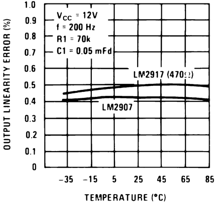 Figure 1. Tachometer Linearity vs Temperature
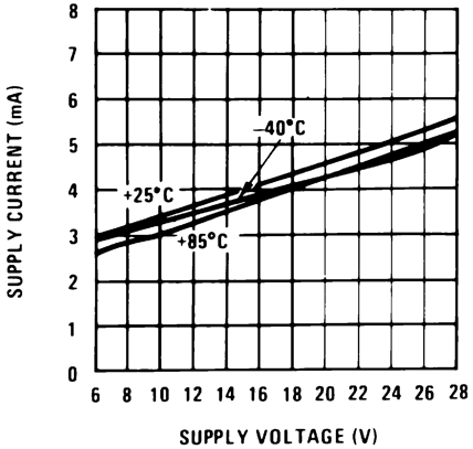 Figure 3. Total Supply Current
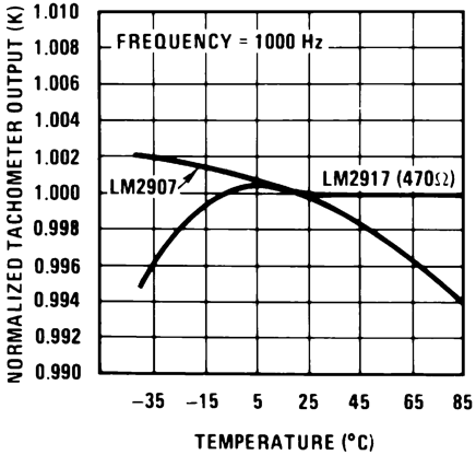 Figure 5. Normalized Tachometer Output (K)
vs Temperature
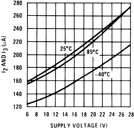 Figure 7. Tachometer Currents I2and I3 vs Supply Voltage
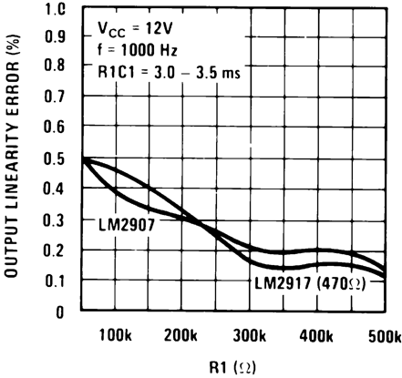 Figure 9. Tachometer Linearity vs R1
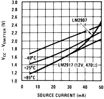 Figure 11. Op Amp Output Transistor Characteristics
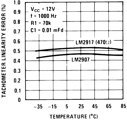 Figure 2. Tachometer Linearity vs Temperature
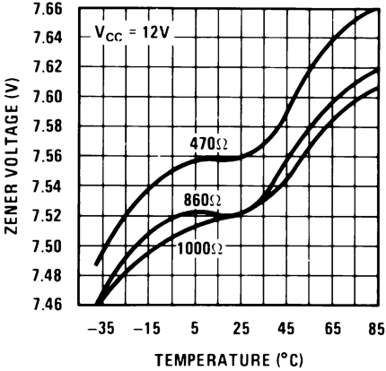 Figure 4. Zener Voltage vs Temperature
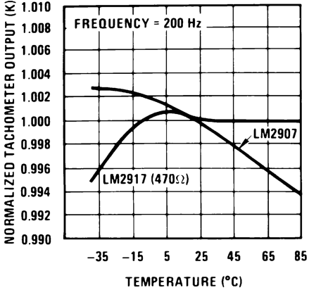 Figure 6. Normalized Tachometer Output (K)
vs Temperature
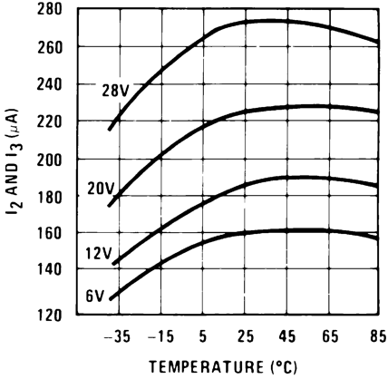 Figure 8. Tachometer Currents I2and I3 vs Temperature
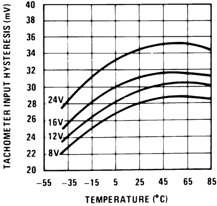 Figure 10. Tachometer Input Hysteresis vs Temperature
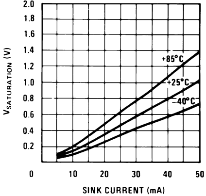 Figure 12. Op Amp Output Transistor Characteristics