SNVS100F March 2000 – July 2014 LM2937
PRODUCTION DATA.
- 1 Features
- 2 Applications
- 3 Description
- 4 Revision History
- 5 Pin Configuration and Functions
-
6 Specifications
- 6.1 Absolute Maximum Ratings
- 6.2 Handling Ratings
- 6.3 Recommended Operating Conditions
- 6.4 Thermal Information
- 6.5 Electrical Characteristics: LM2937-5
- 6.6 Electrical Characteristics: LM2937-8
- 6.7 Electrical Characteristics: LM2937-10
- 6.8 Electrical Characteristics: LM2937-12
- 6.9 Electrical Characteristics: LM2937-15
- 6.10 Typical Characteristics
- 7 Detailed Description
- 8 Application and Implementation
- 9 Power Supply Recommendations
- 10Layout
- 11Device and Documentation Support
- 12Mechanical, Packaging, and Orderable Information
Package Options
Mechanical Data (Package|Pins)
Thermal pad, mechanical data (Package|Pins)
Orderable Information
10 Layout
10.1 Layout Guidelines
The dynamic performance of the LM2937 is dependent on the layout of the PCB. PCB layout practices that are adequate for typical LDO's may degrade the PSRR, noise, or transient performance of the LM2937. Best performance is achieved by placing CIN and COUT on the same side of the PCB as the LM2937, and as close as is practical to the package. The ground connections for CIN and COUT should be back to the LM2937 ground pin using as wide, and as short, of a copper trace as is practical.
Connections using long trace lengths, narrow trace widths, and/or connections through vias should be avoided as these will add parasitic inductances and resistances that will give inferior performance, especially during transient conditions
10.2 Layout Example
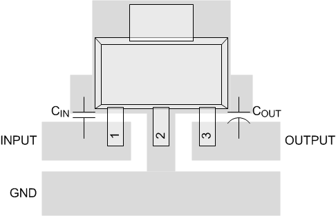 Figure 27. LM2937 SOT-223-4 Layout