SNVS100F March 2000 – July 2014 LM2937
PRODUCTION DATA.
- 1 Features
- 2 Applications
- 3 Description
- 4 Revision History
- 5 Pin Configuration and Functions
-
6 Specifications
- 6.1 Absolute Maximum Ratings
- 6.2 Handling Ratings
- 6.3 Recommended Operating Conditions
- 6.4 Thermal Information
- 6.5 Electrical Characteristics: LM2937-5
- 6.6 Electrical Characteristics: LM2937-8
- 6.7 Electrical Characteristics: LM2937-10
- 6.8 Electrical Characteristics: LM2937-12
- 6.9 Electrical Characteristics: LM2937-15
- 6.10 Typical Characteristics
- 7 Detailed Description
- 8 Application and Implementation
- 9 Power Supply Recommendations
- 10Layout
- 11Device and Documentation Support
- 12Mechanical, Packaging, and Orderable Information
Package Options
Mechanical Data (Package|Pins)
Thermal pad, mechanical data (Package|Pins)
Orderable Information
6 Specifications
6.1 Absolute Maximum Ratings(1)(2)
over operating free-air temperature range (unless otherwise noted)| MIN | MAX | UNIT | ||
|---|---|---|---|---|
| Input voltage (VIN) | Continuous | 26 | V | |
| Transient (t ≤ 100 ms) | 60 | |||
| Internal power dissipation(3) | Internally limited | |||
| Maximum junction temperature | 150 | °C | ||
(1) Stresses beyond those listed under Absolute Maximum Ratings may cause permanent damage to the device. These are stress ratings only, which do not imply functional operation of the device at these or any other conditions beyond those indicated under Recommended Operating Conditions. Exposure to absolute-maximum-rated conditions for extended periods may affect device reliability.
(2) If Military/Aerospace specified devices are required, please contact the Texas Instruments Sales Office/Distributors for availability and specifications.
(3) The maximum allowable power dissipation at any ambient temperature is PMAX = (125°C − TA)/RθJA, where 125 is the maximum junction temperature for operation, TA is the ambient temperature, and RθJA is the junction-to-ambient thermal resistance. If this dissipation is exceeded, the die temperature will rise above 125°C and the electrical specifications do not apply. If the die temperature rises above 150°C, the LM2937 will go into thermal shutdown.
6.2 Handling Ratings
| MIN | MAX | UNIT | |||
|---|---|---|---|---|---|
| Tstg | Storage temperature range | −65 | 150 | °C | |
| V(ESD) | Electrostatic discharge | Human body model (HBM), per ANSI/ESDA/JEDEC JS-001, all pins(1) | –2000 | 2000 | V |
(1) JEDEC document JEP155 states that 500-V HBM allows safe manufacturing with a standard ESD control process.
6.3 Recommended Operating Conditions(1)
over operating free-air temperature range (unless otherwise noted)| MIN | NOM | MAX | UNIT | ||
|---|---|---|---|---|---|
| Junction temperature (TJ) (2) | LM2937ET (NDE), LM2937ES (KTT) | −40 | 125 | °C | |
| LM2937IMP (DCY) | −40 | 85 | |||
| Input voltage (VIN) | VOUT + 1V | 26 | V | ||
(1) Stresses beyond those listed under Absolute Maximum Ratings may cause permanent damage to the device. These are stress ratings only, which do not imply functional operation of the device at these or any other conditions beyond those indicated under Recommended Operating Conditions. Exposure to absolute-maximum-rated conditions for extended periods may affect device reliability.
(2) The maximum allowable power dissipation at any ambient temperature is PMAX = (125°C − TA)/RθJA, where 125°C is the maximum junction temperature for operation, TA is the ambient temperature, and RθJA is the junction-to-ambient thermal resistance. If this dissipation is exceeded, the die temperature will rise above 125°C and the electrical specifications do not apply. If the die temperature rises above 150°C, the LM2937 will go into thermal shutdown.
6.4 Thermal Information
| THERMAL METRIC(1) | LM2937 | UNIT | |||
|---|---|---|---|---|---|
| NDE(2) | KTT | DCY | |||
| 3 PINS | 3 PINS | 4 PINS | |||
| RθJA | Junction-to-ambient thermal resistance | 77.9 | 41.8 | 58.3 | °C/W |
| RθJC(top) | Junction-to-case (top) thermal resistance | 35.5 | 43.5 | 39.2 | |
| RθJB | Junction-to-board thermal resistance | 70.6 | 0.8 | N/A | |
| ψJT | Junction-to-top characterization parameter | 13 | 23.5 | 7 | |
| ψJB | Junction-to-board characterization parameter | 70.6 | 10.3 | 1.6 | |
| RθJC(bot) | Junction-to-case (bottom) thermal resistance | 1 | 22.5 | 22.5 | |
(1) For more information about traditional and new thermal metrics, see the IC Package Thermal Metrics application report, SPRA953.
(2) Thermal information for the TO-220 package is for a free-standing package vertically mounted in the middle of a PCB which is compliant to the JEDEC HIGH-K 2s2p (JESD51-7) specifications. No additional heat sink is attached. See Heatsinking TO-220 Package Parts section for more information.
6.5 Electrical Characteristics: LM2937-5
Unless otherwise specified: VIN = VOUT(NOM) + 5 V; IOUT(MAX) = 500 mA for the TO-220 and DDPAK/TO-263 packages; IOUT(MAX) = 400 mA for the SOT-223 package; and COUT = 10 μF. Conditions and the associated minimum and maximum limits apply over the Recommended Operating temperature range for the specific package, unless otherwise noted.| PARAMETER | CONDITIONS | MIN | TYP | MAX | UNIT |
|---|---|---|---|---|---|
| Output voltage | TA = TJ = 25°C, 5 mA ≤ IOUT ≤ IOUT(MAX) | 4.85 | 5 | 5.15 | V |
| 5 mA ≤ IOUT ≤ IOUT(MAX) | 4.75 | 5 | 5.25 | V | |
| Line regulation | (VOUT + 2 V) ≤ VIN ≤ 26 V, IOUT = 5 mA | 15 | 50 | mV | |
| Load regulation | 5 mA ≤ IOUT ≤ IOUT(MAX) | 5 | 50 | mV | |
| Quiescent Current | (VOUT + 2 V) ≤ VIN ≤ 26 V, IOUT = 5 mA | 2 | 10 | mA | |
| VIN = (VOUT + 5 V), IOUT = IOUT(MAX) | 10 | 20 | mA | ||
| Output noise voltage | 10 Hz to 100 kHz, IOUT = 5 mA | 150 | μVrms | ||
| Long-term stability | 1000 Hrs. | 20 | mV | ||
| Dropout voltage | IOUT = IOUT(MAX) | 0.5 | 1 | V | |
| IOUT = 50 mA | 110 | 250 | mV | ||
| Short-circuit current | 0.6 | 1 | A | ||
| Peak line transient voltage | tf < 100 ms, RL = 100 Ω | 60 | 75 | V | |
| Maximum operational input voltage | 26 | V | |||
| Reverse DC input voltage | VOUT ≥ −0.6 V, RL = 100 Ω | –15 | –30 | V | |
| Reverse transient input voltage | tr < 1 ms, RL = 100 Ω | –50 | –75 | V |
6.6 Electrical Characteristics: LM2937-8
Unless otherwise specified: VIN = VOUT(NOM) + 5 V; IOUT(MAX) = 500 mA for the TO-220 and DDPAK/TO-263 packages; IOUT(MAX) = 400 mA for the SOT-223 package; and COUT = 10 μF. Conditions and the associated Minimum and Maximum limits apply over the Recommended Operating temperature range for the specific package, unless otherwise noted.| PARAMETER | CONDITIONS | MIN | TYP | MAX | UNIT |
|---|---|---|---|---|---|
| Output voltage | TA = TJ = 25°C, 5 mA ≤ IOUT ≤ IOUT(MAX) | 7.76 | 8 | 8.24 | V |
| 5 mA ≤ IOUT ≤ IOUT(MAX) | 7.6 | 8 | 8.4 | V | |
| Line regulation | (VOUT + 2 V) ≤ VIN ≤ 26 V, IOUT = 5 mA | 24 | 80 | mV | |
| Load regulation | 5 mA ≤ IOUT ≤ IOUT(MAX) | 8 | 80 | mV | |
| Quiescent Current | (VOUT + 2 V) ≤ VIN ≤ 26 V, IOUT = 5 mA | 2 | 10 | mA | |
| VIN = (VOUT + 5 V), IOUT = IOUT(MAX) | 10 | 20 | mA | ||
| Output noise voltage | 10 Hz to 100 kHz, IOUT = 5 mA | 240 | μVrms | ||
| Long-term stability | 1000 Hrs. | 32 | mV | ||
| Dropout voltage | IOUT = IOUT(MAX) | 0.5 | 1 | V | |
| IOUT = 50 mA | 110 | 250 | mV | ||
| Short-circuit current | 0.6 | 1 | A | ||
| Peak line transient voltage | tf < 100 ms, RL = 100 Ω | 60 | 75 | V | |
| Maximum operational input voltage | 26 | V | |||
| Reverse DC input voltage | VOUT ≥ −0.6 V, RL = 100 Ω | –15 | –30 | V | |
| Reverse transient input voltage | tr < 1 ms, RL = 100 Ω | –50 | –75 | V |
6.7 Electrical Characteristics: LM2937-10
Unless otherwise specified: VIN = VOUT(NOM) + 5 V; IOUT(MAX) = 500 mA for the TO-220 and DDPAK/TO-263 packages; IOUT(MAX) = 400 mA for the SOT-223 package; and COUT = 10 μF. Conditions and the associated Minimum and Maximum limits apply over the Recommended Operating temperature range for the specific package, unless otherwise noted.| PARAMETER | CONDITIONS | MIN | TYP | MAX | UNIT |
|---|---|---|---|---|---|
| Output voltage | TA = TJ = 25°C, 5 mA ≤ IOUT ≤ IOUT(MAX) | 9.7 | 10 | 10.3 | V |
| 5 mA ≤ IOUT ≤ IOUT(MAX) | 9.5 | 10 | 10.5 | V | |
| Line regulation | (VOUT + 2V) ≤ VIN ≤ 26V, IOUT = 5 mA | 30 | 100 | mV | |
| Load regulation | 5 mA ≤ IOUT ≤ IOUT(MAX) | 10 | 100 | mV | |
| Quiescent Current | (VOUT + 2V) ≤ VIN ≤ 26V, IOUT = 5 mA | 2 | 10 | mA | |
| VIN = (VOUT + 5V), IOUT = IOUT(MAX) | 10 | 20 | mA | ||
| Output noise voltage | 10 Hz to 100 kHz, IOUT = 5 mA | 300 | μVrms | ||
| Long-term stability | 1000 Hrs. | 40 | mV | ||
| Dropout voltage | IOUT = IOUT(MAX) | 0.5 | 1 | V | |
| IOUT = 50 mA | 110 | 250 | mV | ||
| Short-circuit current | 0.6 | 1 | A | ||
| Peak line transient voltage | tf < 100 ms, RL = 100 Ω | 60 | 75 | V | |
| Maximum operational input voltage | 26 | V | |||
| Reverse DC input voltage | VOUT ≥ −0.6 V, RL = 100 Ω | –15 | –30 | V | |
| Reverse transient input voltage | tr < 1 ms, RL = 100 Ω | –50 | –75 | V |
6.8 Electrical Characteristics: LM2937-12
Unless otherwise specified: VIN = VOUT(NOM) + 5 V; IOUT(MAX) = 500 mA for the TO-220 and DDPAK/TO-263 packages; IOUT(MAX) = 400 mA for the SOT-223 package; and COUT = 10 μF. Conditions and the associated Minimum and Maximum limits apply over the Recommended Operating temperature range for the specific package, unless otherwise noted.| PARAMETER | CONDITIONS | MIN | TYP | MAX | UNIT |
|---|---|---|---|---|---|
| Output voltage | TA = TJ = 25°C, 5 mA ≤ IOUT ≤ IOUT(MAX) | 11.64 | 12 | 12.36 | V |
| 5 mA ≤ IOUT ≤ IOUT(MAX) | 11.4 | 12 | 12.6 | V | |
| Line regulation | (VOUT + 2V) ≤ VIN ≤ 26V, IOUT = 5 mA | 36 | 120 | mV | |
| Load regulation | 5 mA ≤ IOUT ≤ IOUT(MAX) | 12 | 120 | mV | |
| Quiescent Current | (VOUT + 2V) ≤ VIN ≤ 26V, IOUT = 5 mA | 2 | 10 | mA | |
| VIN = (VOUT + 5V), IOUT = IOUT(MAX) | 10 | 20 | mA | ||
| Output noise voltage | 10 Hz to 100 kHz, IOUT = 5 mA | 360 | μVrms | ||
| Long-term stability | 1000 Hrs. | 44 | mV | ||
| Dropout voltage | IOUT = IOUT(MAX) | 0.5 | 1 | V | |
| IOUT = 50 mA | 110 | 250 | mV | ||
| Short-circuit current | 0.6 | 1 | A | ||
| Peak line transient voltage | tf < 100 ms, RL = 100 Ω | 60 | 75 | V | |
| Maximum operational input voltage | 26 | V | |||
| Reverse DC input voltage | VOUT ≥ −0.6 V, RL = 100 Ω | –15 | –30 | V | |
| Reverse transient input voltage | tr < 1 ms, RL = 100 Ω | –50 | –75 | V |
6.9 Electrical Characteristics: LM2937-15
Unless otherwise specified: VIN = VOUT(NOM) + 5 V; IOUT(MAX) = 500 mA for the TO-220 and DDPAK/TO-263 packages; IOUT(MAX) = 400 mA for the SOT-223 package; and COUT = 10 μF. Conditions and the associated Minimum and Maximum limits apply over the Recommended Operating temperature range for the specific package, unless otherwise noted.| PARAMETER | CONDITIONS | MIN | TYP | MAX | UNIT |
|---|---|---|---|---|---|
| Output voltage | TA = TJ = 25°C, 5 mA ≤ IOUT ≤ IOUT(MAX) | 14.55 | 15 | 15.45 | V |
| 5 mA ≤ IOUT ≤ IOUT(MAX) | 14.25 | 15 | 15.75 | V | |
| Line regulation | (VOUT + 2V) ≤ VIN ≤ 26V, IOUT = 5 mA | 45 | 150 | mV | |
| Load regulation | 5 mA ≤ IOUT ≤ IOUT(MAX) | 15 | 150 | mV | |
| Quiescent Current | (VOUT + 2V) ≤ VIN ≤ 26V, IOUT = 5 mA | 2 | 10 | mA | |
| VIN = (VOUT + 5V), IOUT = IOUT(MAX) | 10 | 20 | mA | ||
| Output noise voltage | 10 Hz to 100 kHz, IOUT = 5 mA | 450 | μVrms | ||
| Long-term stability | 1000 Hrs. | 56 | mV | ||
| Dropout voltage | IOUT = IOUT(MAX) | 0.5 | 1 | V | |
| IOUT = 50 mA | 110 | 250 | mV | ||
| Short-circuit current | 0.6 | 1 | A | ||
| Peak line transient voltage | tf < 100 ms, RL = 100 Ω | 60 | 75 | V | |
| Maximum operational input voltage | 26 | V | |||
| Reverse DC input voltage | VOUT ≥ −0.6 V, RL = 100 Ω | –15 | –30 | V | |
| Reverse transient input voltage | tr < 1 ms, RL = 100 Ω | –50 | –75 | V |
6.10 Typical Characteristics
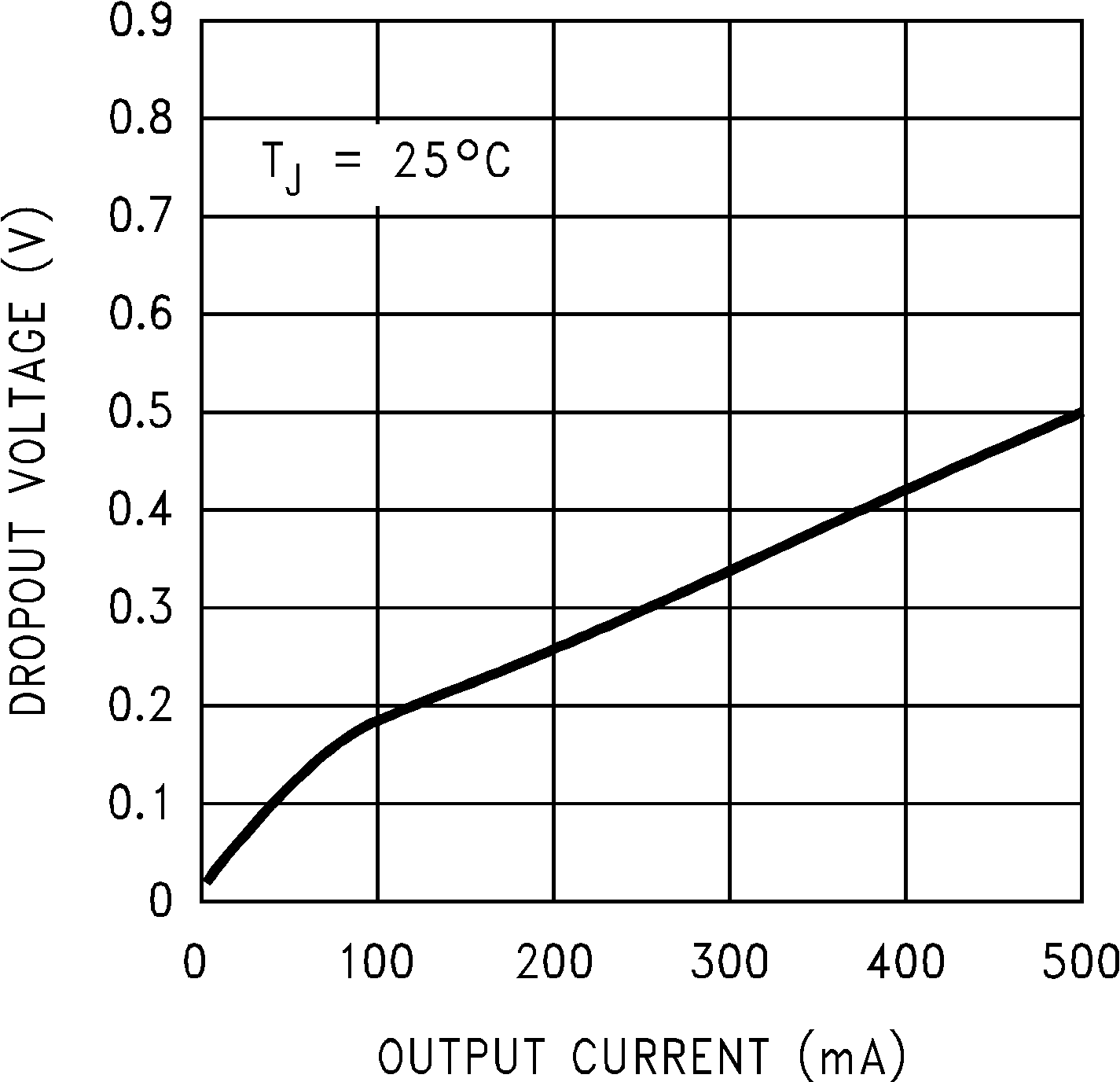 Figure 1. Dropout Voltage vs. Output Current
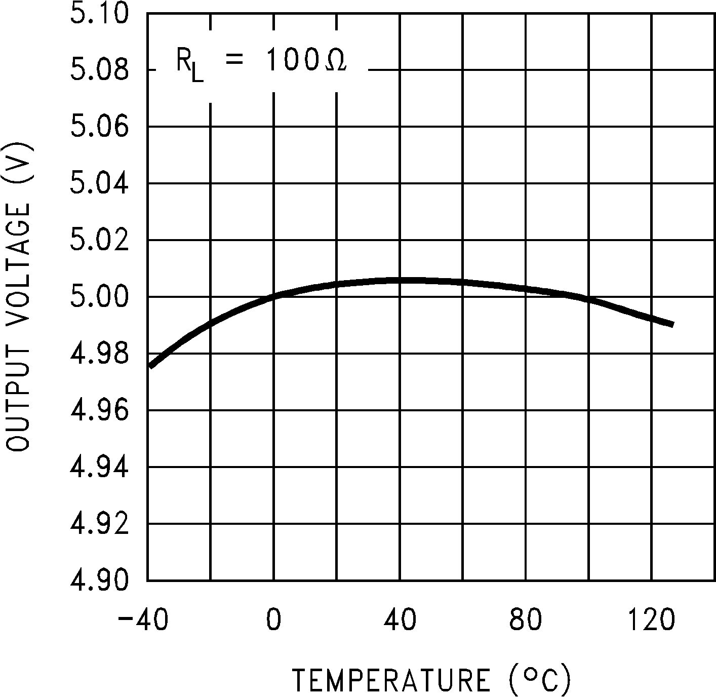 Figure 3. Output Voltage vs. Temperature
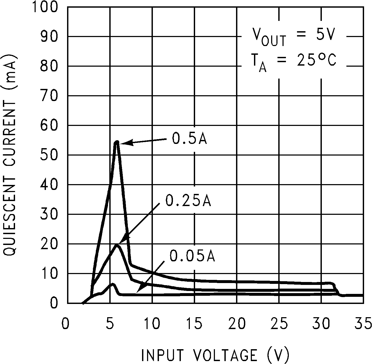 Figure 5. Quiescent Current vs. Input Voltage
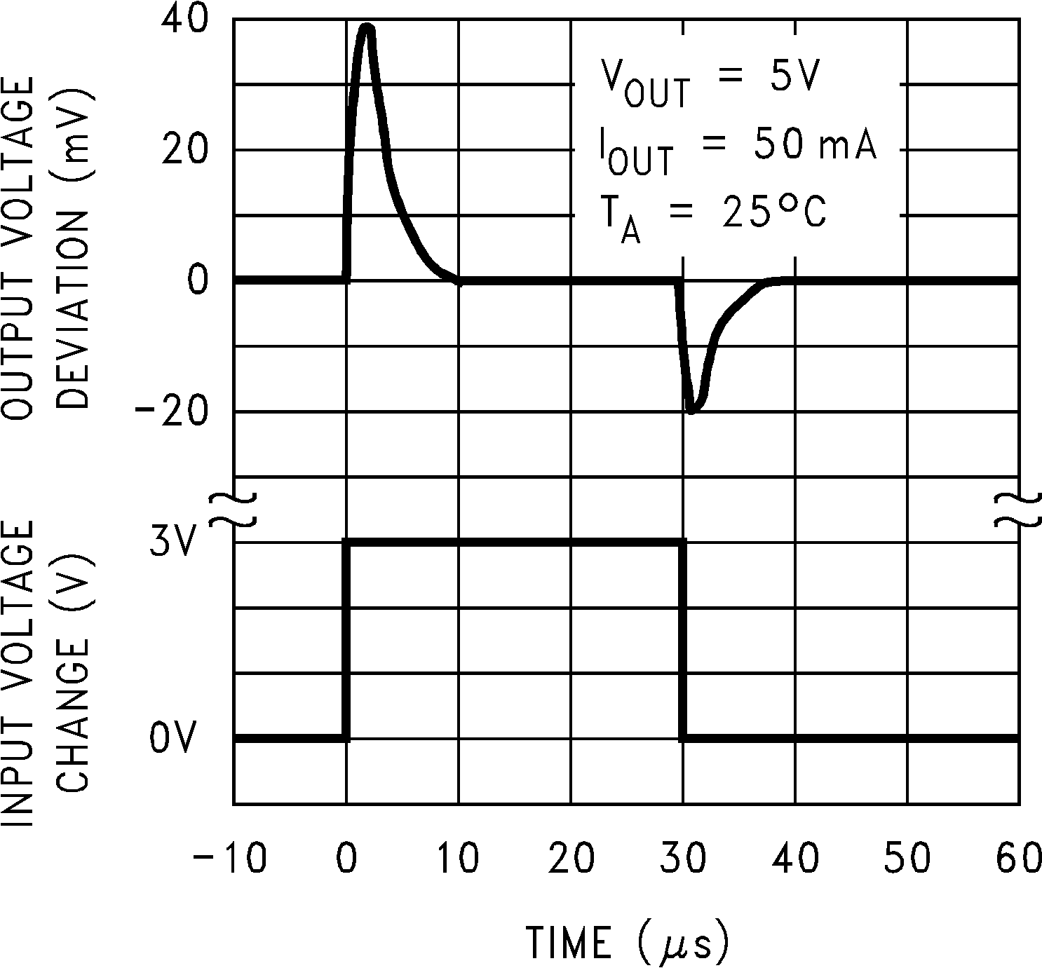 Figure 7. Line Transient Response
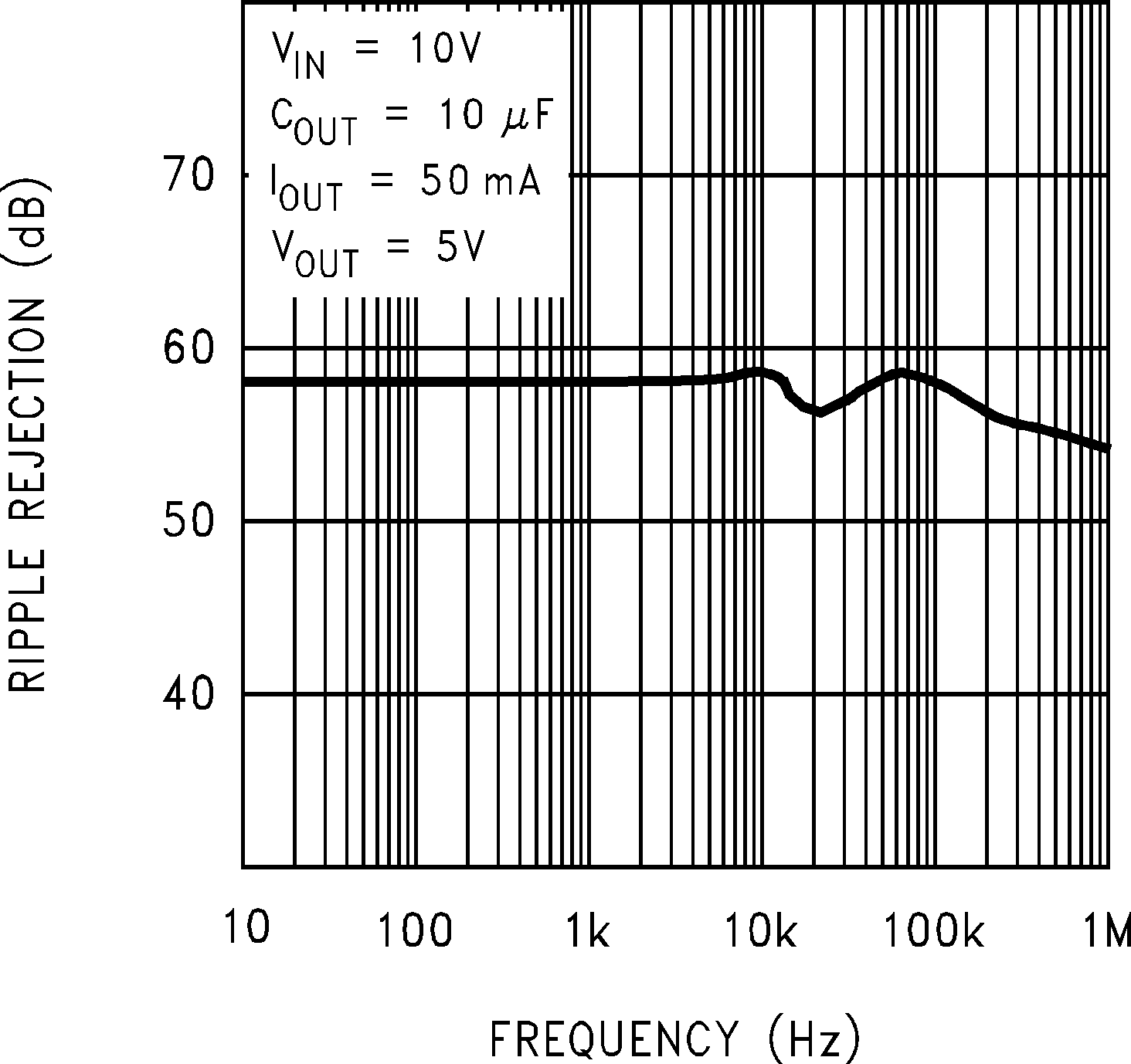 Figure 9. Ripple Rejection
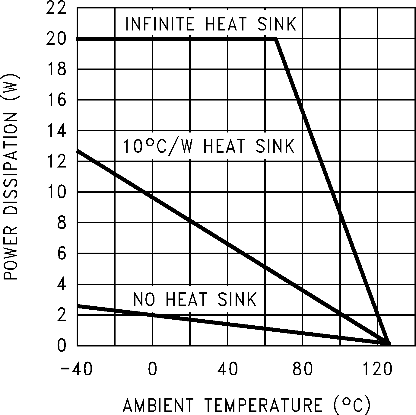 Figure 11. Maximum Power Dissipation (TO-220)1
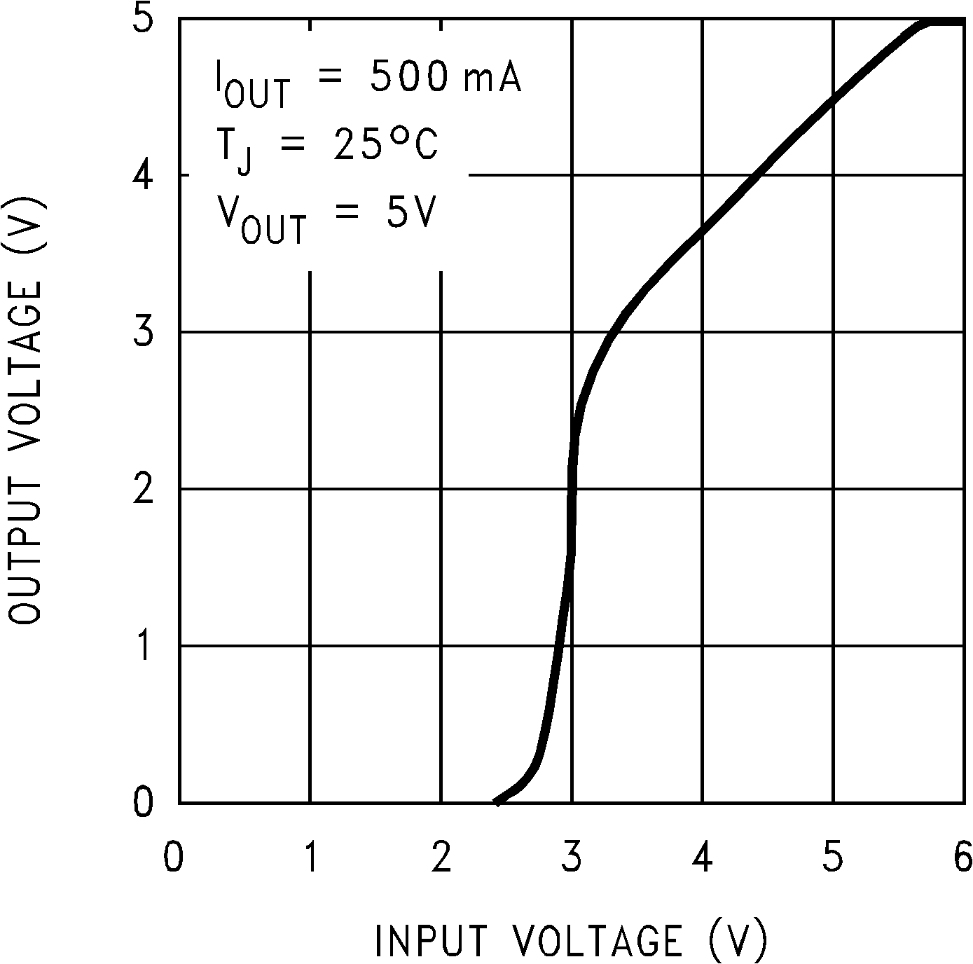 Figure 13. Low-Voltage Behavior
 Figure 15. Output at Voltage Extremes
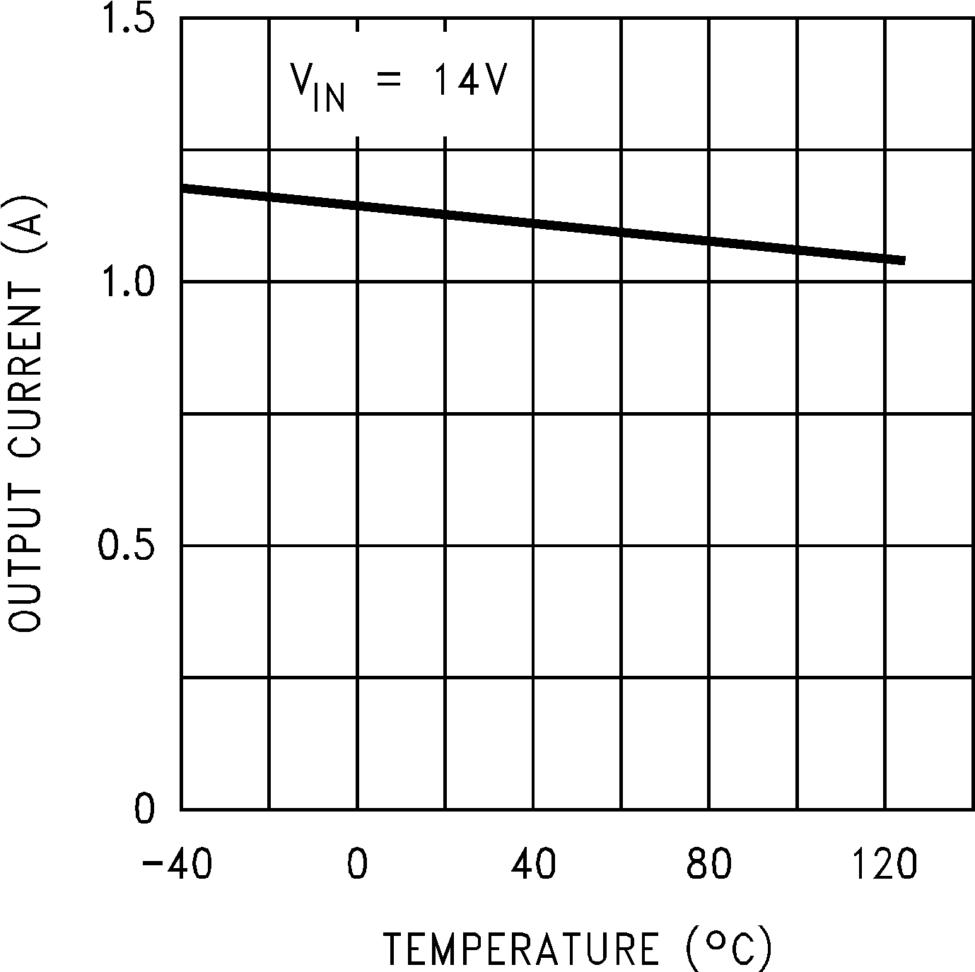 Figure 17. Peak Output Current
 Figure 2. Dropout Voltage vs. Temperature
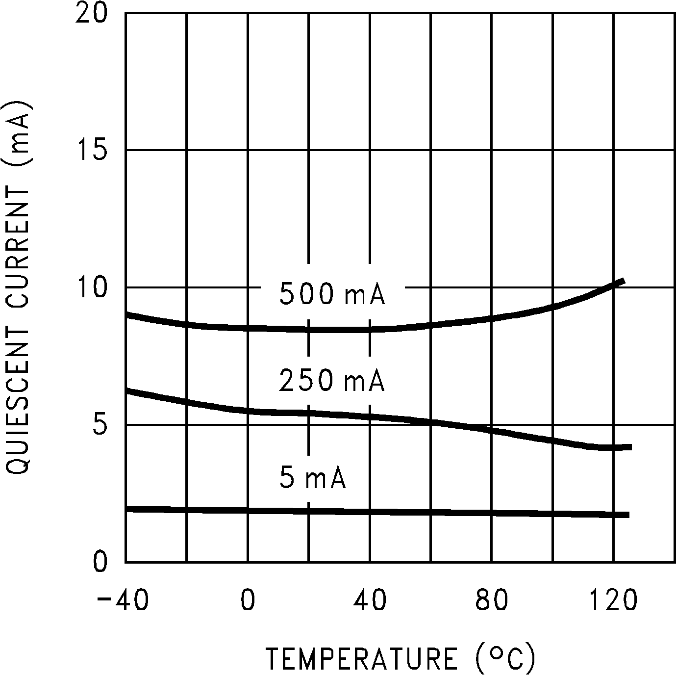 Figure 4. Quiescent Current vs. Temperature
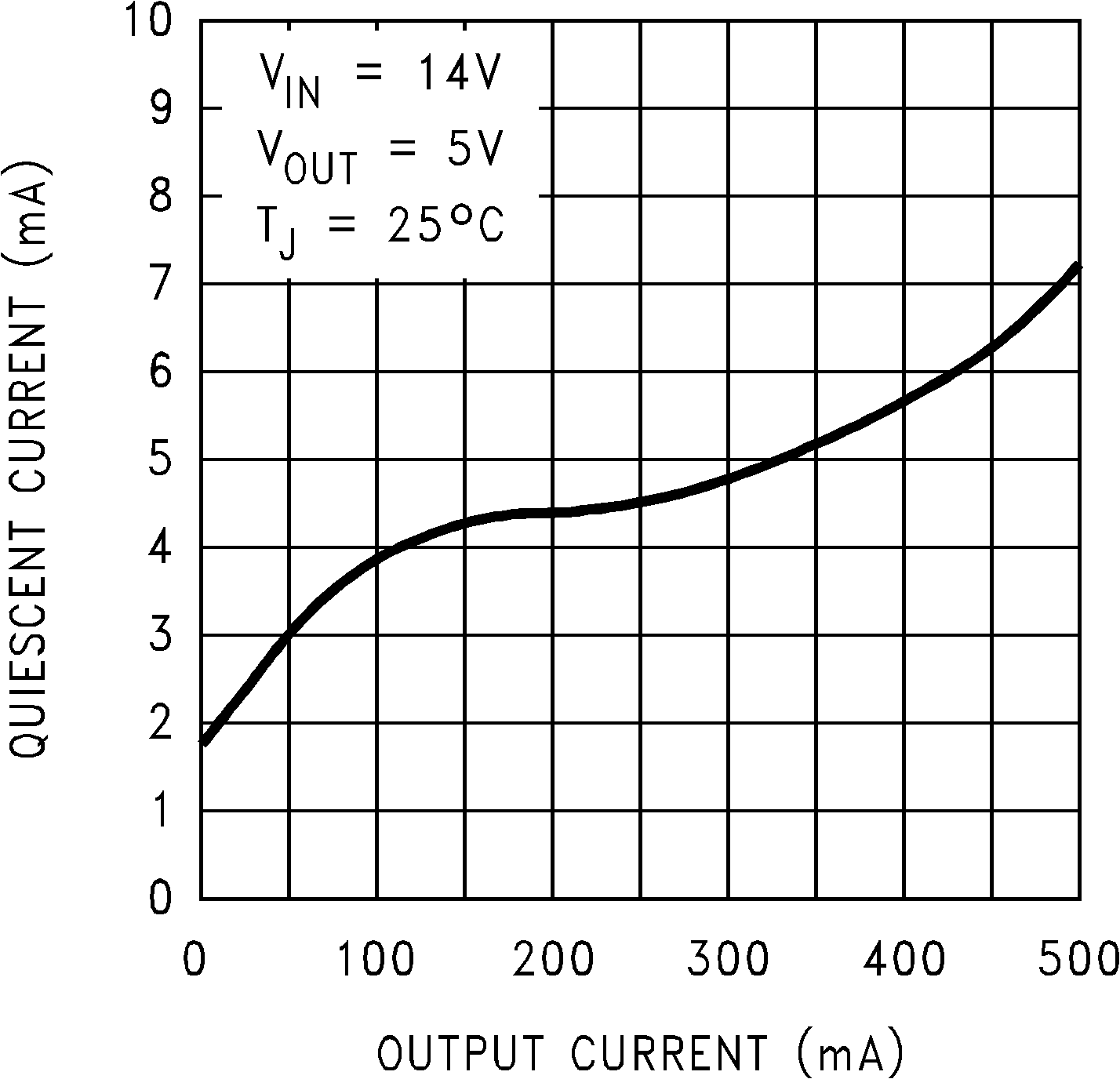 Figure 6. Quiescent Current vs. Output Current
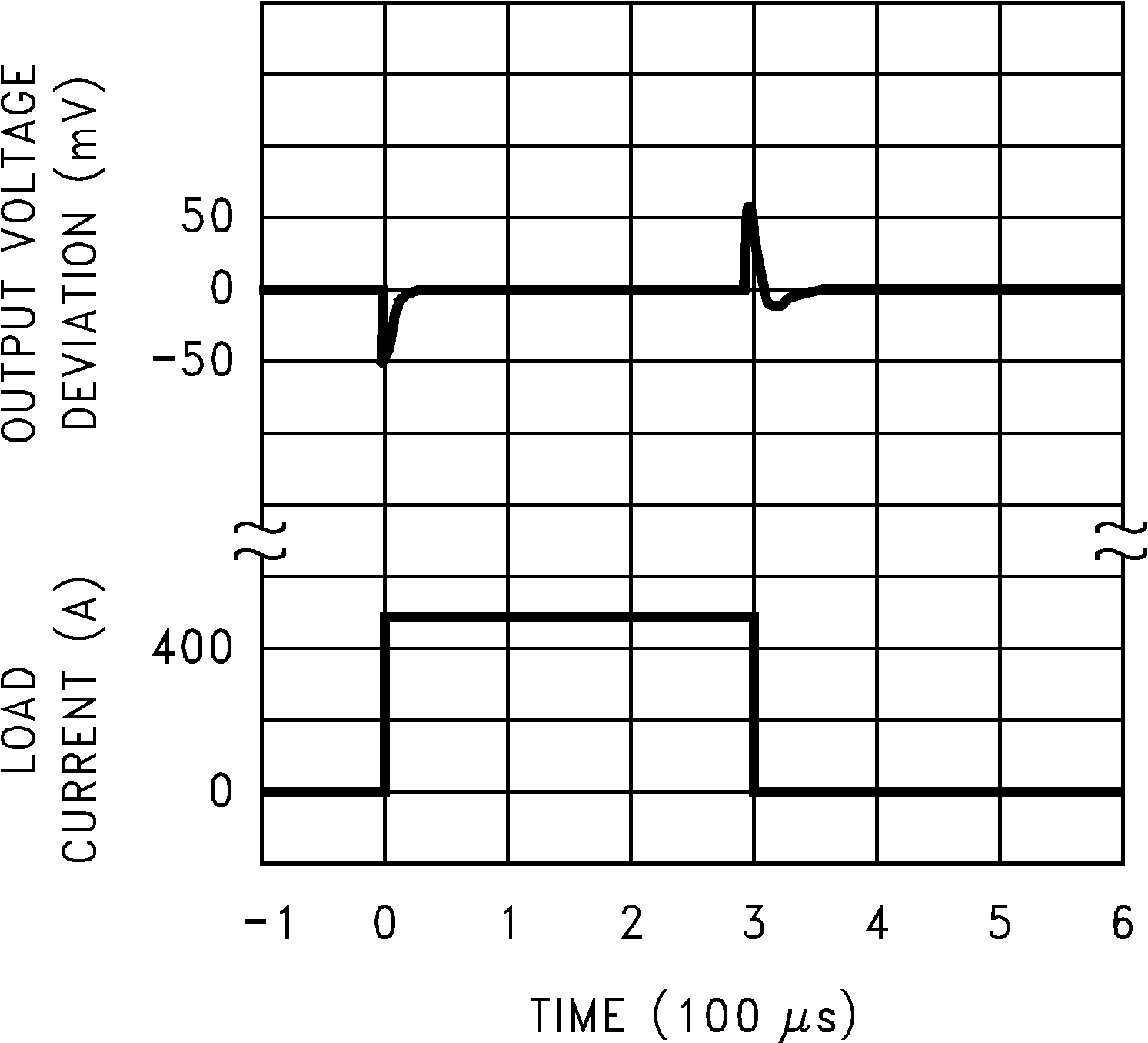 Figure 8. Load Transient Response
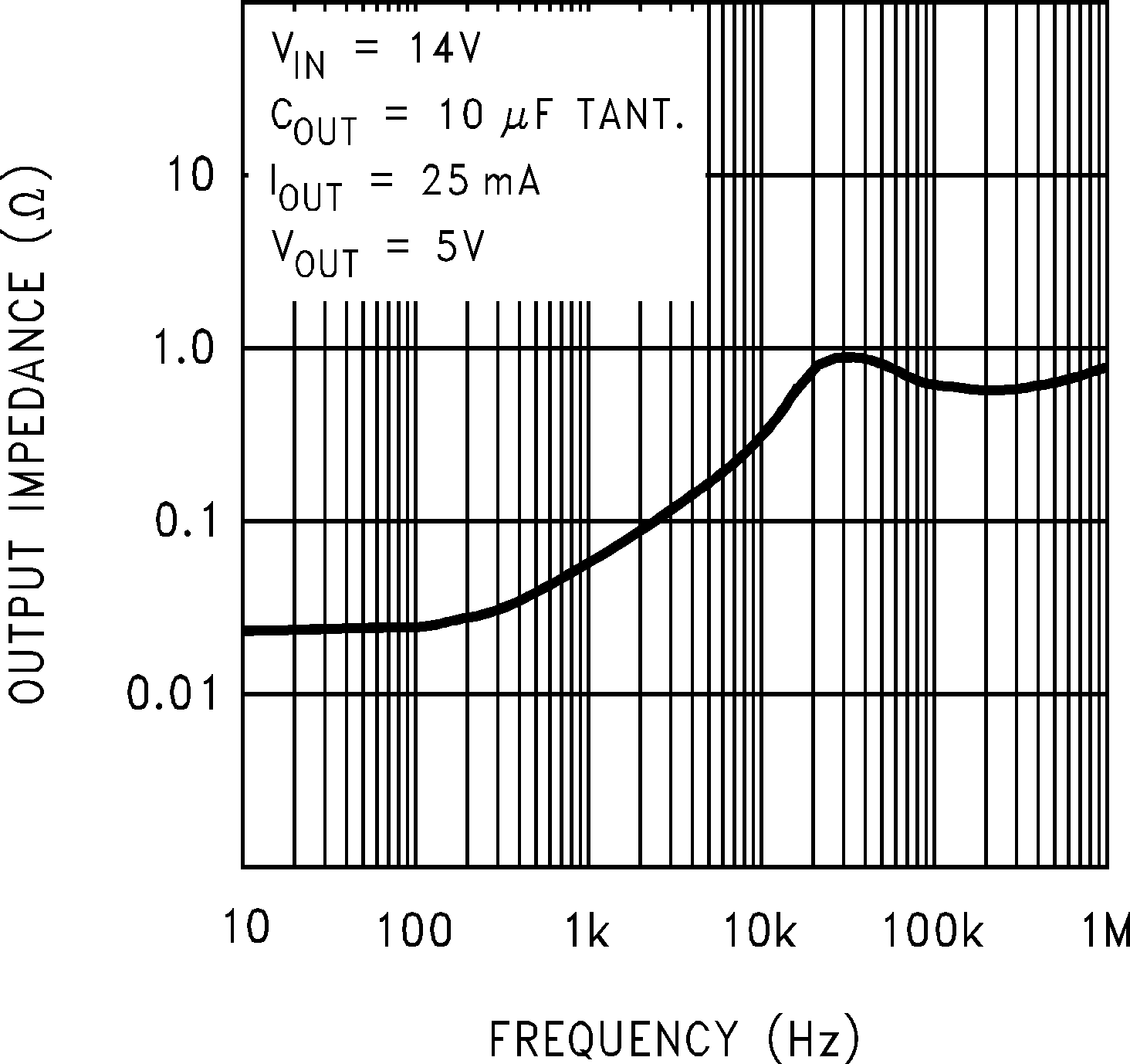 Figure 10. Output Impedence
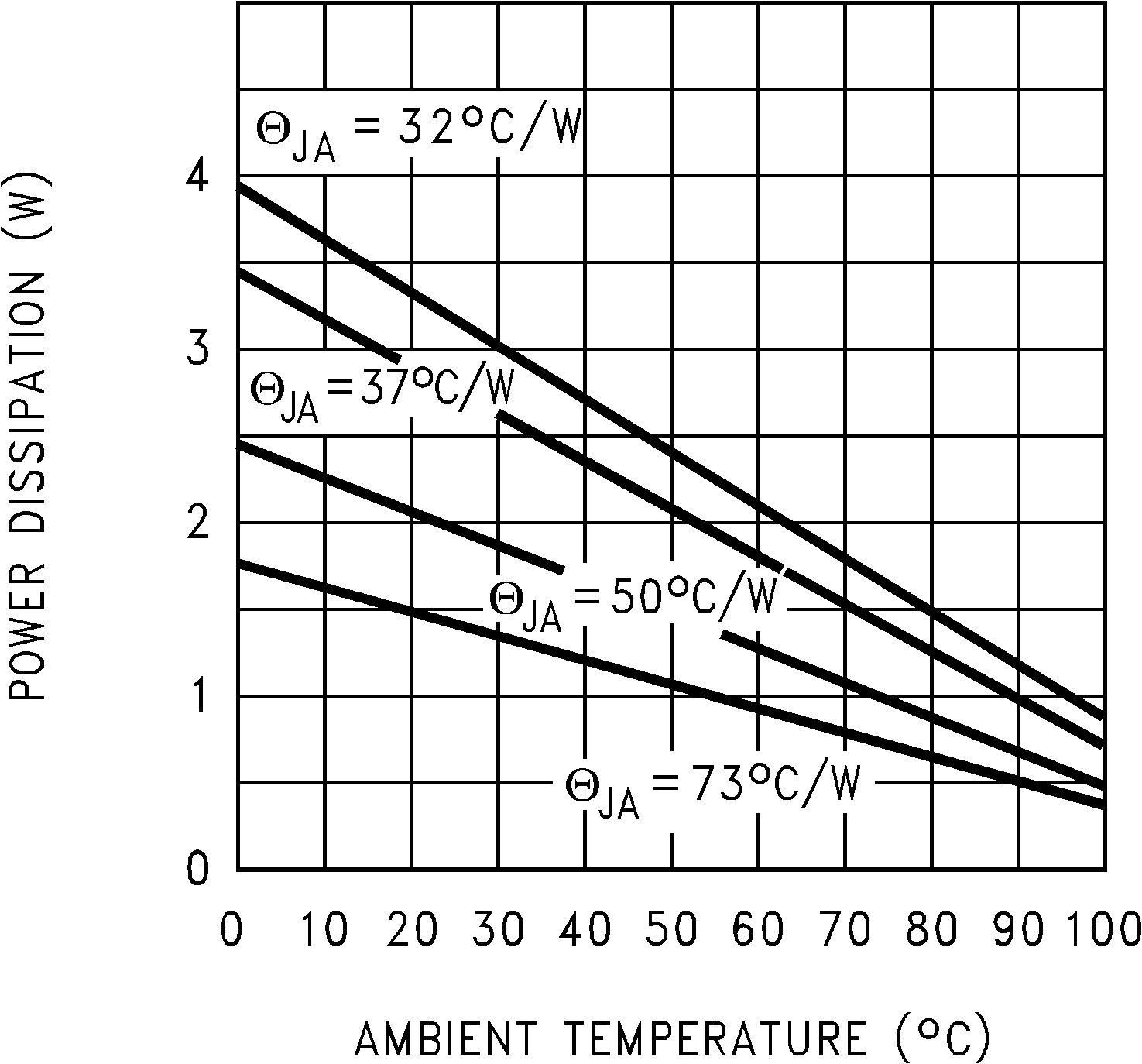
1. The maximum allowable power dissipation at any ambient temperature is PMAX = (125°C − TA)/RθJA, where 125 is the maximum junction temperature for operation, TA is the ambient temperature, and RθJA is the junction-to-ambient thermal resistance. If this dissipation is exceeded, the die temperature will rise above 125°C and the electrical specifications do not apply. If the die temperature rises above 150°C, the LM2937 will go into thermal shutdown.
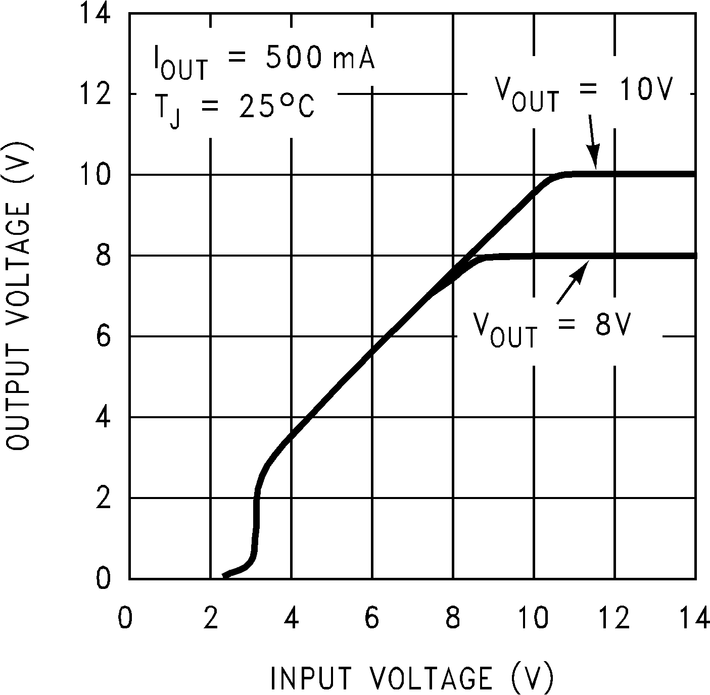 Figure 14. Low-Voltage Behavior
 Figure 16. Output Capacitor ESR