SNVS515I September 2007 – January 2018 LM3102
PRODUCTION DATA.
- 1 Features
- 2 Applications
- 3 Description
- 4 Revision History
- 5 Pin Configuration and Functions
- 6 Specifications
- 7 Detailed Description
- 8 Application and Implementation
- 9 Power Supply Recommendations
- 10Layout
- 11Device and Documentation Support
- 12Mechanical, Packaging, and Orderable Information
Package Options
Refer to the PDF data sheet for device specific package drawings
Mechanical Data (Package|Pins)
- YPA|28
- PWP|20
Thermal pad, mechanical data (Package|Pins)
- PWP|20
Orderable Information
7.3.6 Current Limit
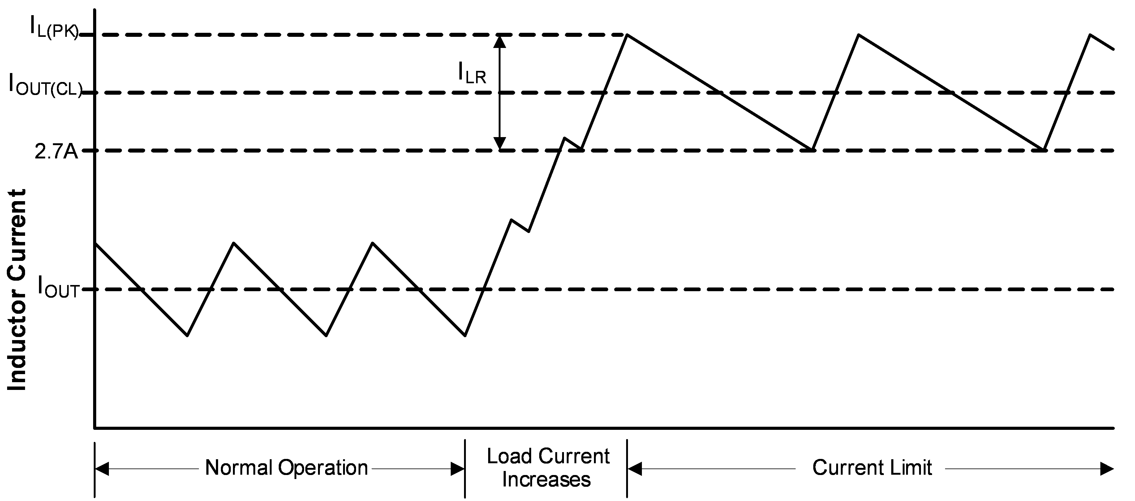
Current limit detection is carried out during the OFF-time by monitoring the re-circulating current through the synchronous MOSFET. Referring to the Functional Block Diagram, when the main MOSFET is turned off, the inductor current flows through the load, the PGND pin and the internal synchronous MOSFET. If this current exceeds 2.7 A, the current limit comparator toggles, and as a result disabling the start of the next ON-time period. The next switching cycle starts when the re-circulating current falls back below 2.7 A (and the voltage at the FB pin is below 0.8V). The inductor current is monitored during the ON-time of the synchronous MOSFET. As long as the inductor current exceeds 2.7 A, the main MOSFET will remain inhibited to achieve current limit. The operating frequency is lower during current limit due to a longer OFF-time.
Figure 20 illustrates an inductor current waveform. On average, the output current IOUT is the same as the inductor current IL, which is the average of the rippled inductor current. In case of current limit (the current limit portion of Figure 20), the next ON-time will not initiate until that the current drops below 2.7 A (assume the voltage at the FB pin is lower than 0.8 V). During each ON-time the current ramps up an amount equal to:

During current limit, the LM3102 operates in a constant current mode with an average output current IOUT(CL) equal to 2.7 A + ILR / 2.
 Figure 20. Inductor Current - Current Limit Operation