SNVS515I September 2007 – January 2018 LM3102
PRODUCTION DATA.
- 1 Features
- 2 Applications
- 3 Description
- 4 Revision History
- 5 Pin Configuration and Functions
- 6 Specifications
- 7 Detailed Description
- 8 Application and Implementation
- 9 Power Supply Recommendations
- 10Layout
- 11Device and Documentation Support
- 12Mechanical, Packaging, and Orderable Information
Package Options
Refer to the PDF data sheet for device specific package drawings
Mechanical Data (Package|Pins)
- YPA|28
- PWP|20
Thermal pad, mechanical data (Package|Pins)
- PWP|20
Orderable Information
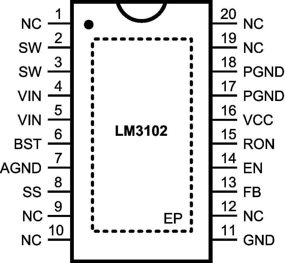
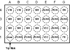
5 Pin Configuration and Functions
PWP Package
20-Pin HTSSOP
Top View

YPA Package
28–Ball DSBGA
Top View

Pin Functions
| PIN | TYPE | DESCRIPTION | ||
|---|---|---|---|---|
| NAME | PIN NO. | BALL NO. | ||
| N/C | 1 | — | — | No Connection |
| 9 | ||||
| 10 | ||||
| 12 | ||||
| 19 | ||||
| 20 | ||||
| SW | 2 | A2 | Power | Switching Node |
| A3 | ||||
| B2 | ||||
| B3 | ||||
| C2 | ||||
| 3 | C3 | |||
| D2 | ||||
| D3 | ||||
| D4 | ||||
| VIN | 4 | A4 | Power | Input supply voltage |
| 5 | B4 | |||
| BST | 6 | C4 | Power | Connection for bootstrap capacitor |
| AGND | 7 | E3 | Ground | Analog Ground |
| E4 | ||||
| F1 | ||||
| F2 | ||||
| F3 | ||||
| G3 | ||||
| SS | 8 | G2 | Analog | Soft-Start |
| GND | 11 | — | Ground | Ground |
| FB | 13 | G1 | Analog | Feedback |
| EN | 14 | G4 | Analog | Enable |
| RON | 15 | F4 | Analog | ON-time Control |
| VCC | 16 | E1 | Power | Start-up regulator Output |
| E2 | ||||
| PGND | 17 | A1 | Ground | Power Ground |
| B1 | ||||
| 18 | C1 | |||
| D1 | ||||
| EP | EP | — | Ground | Exposed Pad |