SNVS515I September 2007 – January 2018 LM3102
PRODUCTION DATA.
- 1 Features
- 2 Applications
- 3 Description
- 4 Revision History
- 5 Pin Configuration and Functions
- 6 Specifications
- 7 Detailed Description
- 8 Application and Implementation
- 9 Power Supply Recommendations
- 10Layout
- 11Device and Documentation Support
- 12Mechanical, Packaging, and Orderable Information
Package Options
Refer to the PDF data sheet for device specific package drawings
Mechanical Data (Package|Pins)
- YPA|28
- PWP|20
Thermal pad, mechanical data (Package|Pins)
- PWP|20
Orderable Information
7.3.8 Soft-Start
The soft-start feature allows the converter to gradually reach a steady-state operating point, thereby reducing startup stresses and current surges. Upon turnon, after VCC reaches the undervoltage threshold, an 8-µA internal current source charges up an external capacitor CSS connecting to the SS pin. The ramping voltage at the SS pin (and the non-inverting input of the regulation comparator as well) ramps up the output voltage VOUT in a controlled manner.
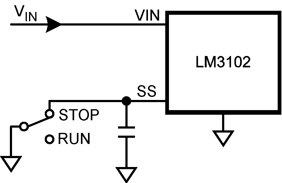
An internal switch grounds the SS pin if any of the following three cases happens: (i) VCC is below the UVLO threshold; (ii) a thermal shutdown occurs; or (iii) the EN pin is grounded. Alternatively, the output voltage can be shut off by connecting the SS pin to ground using an external switch. Releasing the switch allows the SS pin to ramp up and the output voltage to return to normal. The shutdown configuration is shown in Figure 21.
 Figure 21. Alternate Shutdown Implementation