SNVS515I September   2007  – January 2018 LM3102

PRODUCTION DATA.  

  1. Features
  2. Applications
  3. Description
    1.     Device Images
      1.      Typical Application Schematic
      2.      Efficiency vs Load Current (VOUT = 3.3 V)
  4. Revision History
  5. Pin Configuration and Functions
    1.     Pin Functions
  6. Specifications
    1. 6.1 Absolute Maximum Ratings
    2. 6.2 ESD Ratings
    3. 6.3 Recommended Operating Conditions
    4. 6.4 Thermal Information
    5. 6.5 Electrical Characteristics
    6. 6.6 Typical Characteristics
  7. Detailed Description
    1. 7.1 Overview
    2. 7.2 Functional Block Diagram
    3. 7.3 Feature Description
      1. 7.3.1  COT Control Circuit Overview
      2. 7.3.2  Start-Up Regulator (VCC)
      3. 7.3.3  Regulation Comparator
      4. 7.3.4  Zero Coil Current Detect
      5. 7.3.5  Overvoltage Comparator
      6. 7.3.6  Current Limit
      7. 7.3.7  N-Channel MOSFET and Driver
      8. 7.3.8  Soft-Start
      9. 7.3.9  Thermal Protection
      10. 7.3.10 Thermal Derating
    4. 7.4 Device Functional Modes
      1. 7.4.1 ON-Time Timer, Shutdown
  8. Application and Implementation
    1. 8.1 Application Information
    2. 8.2 Typical Application
      1. 8.2.1 Design Requirements
      2. 8.2.2 Detailed Design Procedure
        1. 8.2.2.1 Design Steps for the LM3102 Application
        2. 8.2.2.2 External Components
      3. 8.2.3 Application Curve
    3. 8.3 System Examples
  9. Power Supply Recommendations
  10. 10Layout
    1. 10.1 Layout Guidelines
    2. 10.2 Layout Example
  11. 11Device and Documentation Support
    1. 11.1 Community Resources
    2. 11.2 Trademarks
    3. 11.3 Electrostatic Discharge Caution
    4. 11.4 Glossary
  12. 12Mechanical, Packaging, and Orderable Information

Package Options

Refer to the PDF data sheet for device specific package drawings

Mechanical Data (Package|Pins)
  • YPA|28
  • PWP|20
Thermal pad, mechanical data (Package|Pins)
Orderable Information

Thermal Derating

The LM3102 can supply 2.5 A below an ambient temperature of 100°C. Under worst-case operation, with either input voltage up to 42 V, operating frequency up to 1 MHz, or voltage of the RON pin below the absolute maximum of 7 V, the LM3102 can deliver a minimum of 1.9-A output current without thermal shutdown with a PCB ground plane copper area of 40 cm2, 2 oz/Cu. Figure 22 shows a thermal derating curve for the minimum output current without thermal shutdown against ambient temperature up to 125°C. Obtaining 2.5-A output current is possible by increasing the PCB ground plane area, or reducing the input voltage or operating frequency.
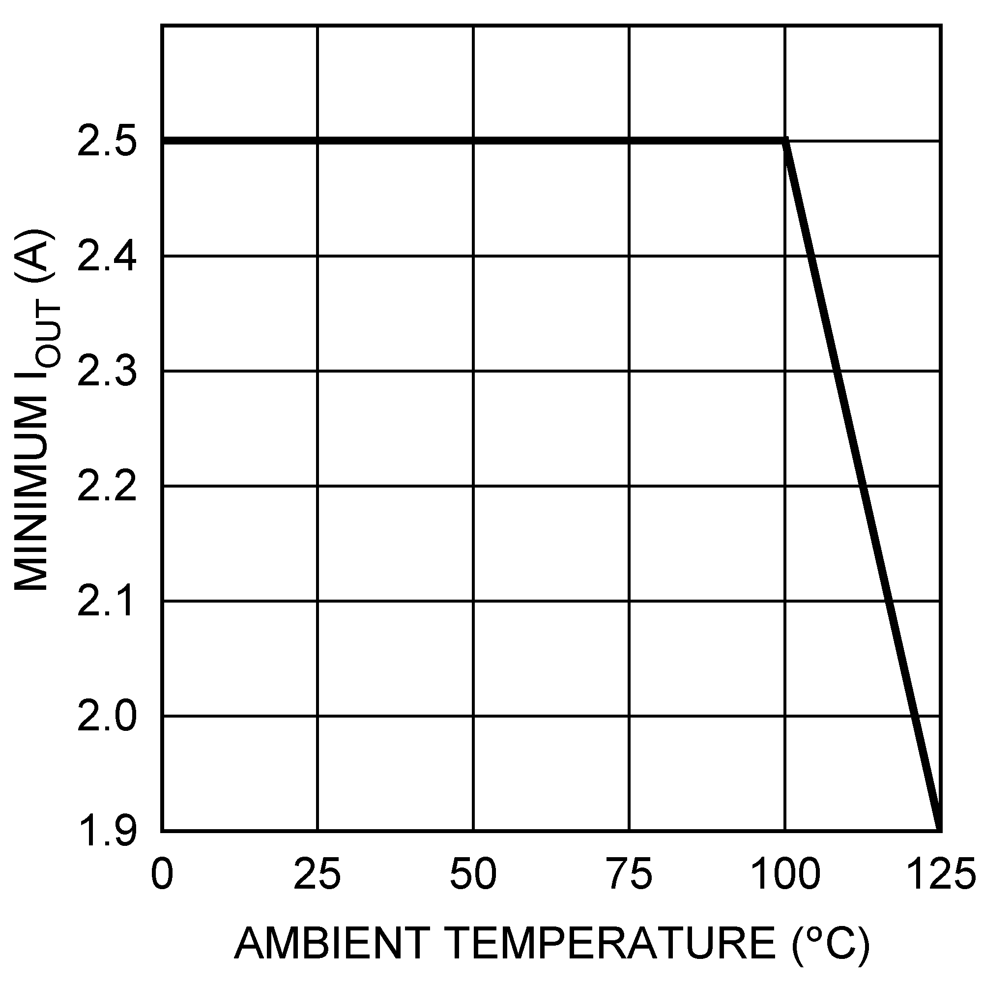
LM3102 30021340.pngFigure 22. Thermal Derating Curve