SNVSAC2A March   2015  – June 2020 LM317A

PRODUCTION DATA.  

  1. Features
  2. Applications
    1.     Typical Application
  3. Description
    1.     Revision History
  4. Device Comparison Table
  5. Pin Configuration and Functions
    1.     Pin Functions
  6. Specifications
    1. 6.1 Absolute Maximum Ratings
    2. 6.2 ESD Ratings
    3. 6.3 Recommended Operating Conditions
    4. 6.4 Thermal Information
    5. 6.5 Electrical Characteristics
    6. 6.6 Typical Characteristics
  7. Detailed Description
    1. 7.1 Overview
    2. 7.2 Functional Block Diagram
    3. 7.3 Feature Description
      1. 7.3.1 Load Regulation
    4. 7.4 Device Functional Modes
      1. 7.4.1 External Capacitors
      2. 7.4.2 Protection Diodes
  8. Application and Implementation
    1. 8.1 Application Information
    2. 8.2 Typical Applications
      1. 8.2.1  1.25-V to 25-V Adjustable Regulator
        1. 8.2.1.1 Design Requirements
        2. 8.2.1.2 Detailed Design Procedure
        3. 8.2.1.3 Application Curve
      2. 8.2.2  5-V Logic Regulator With Electronic Shutdown
      3. 8.2.3  Slow Turnon 15-V Regulator
      4. 8.2.4  Adjustable Regulator With Improved Ripple Rejection
      5. 8.2.5  High-Stability 10-V Regulator
      6. 8.2.6  High-Current Adjustable Regulator
      7. 8.2.7  Emitter-Follower Current Amplifier
      8. 8.2.8  1-A Current Regulator
      9. 8.2.9  Common-Emitter Amplifier
      10. 8.2.10 Low-Cost 3-A Switching Regulator
      11. 8.2.11 Current-Limited Voltage Regulator
      12. 8.2.12 Adjusting Multiple On-Card Regulators With Single Control
      13. 8.2.13 AC Voltage Regulator
      14. 8.2.14 12-V Battery Charger
      15. 8.2.15 Adjustable 4-A Regulator
      16. 8.2.16 Current-Limited 6-V Charger
      17. 8.2.17 Digitally-Selected Outputs
  9. Power Supply Recommendations
  10. 10Layout
    1. 10.1 Layout Guidelines
      1. 10.1.1 Thermal Considerations
        1. 10.1.1.1 Heatsink Requirements
        2. 10.1.1.2 Heatsinking Surface Mount Packages
          1. 10.1.1.2.1 Heatsinking the SOT-223 (DCY) Package
          2. 10.1.1.2.2 Heatsinking the TO-252 (NDP) Package
    2. 10.2 Layout Examples
  11. 11Device and Documentation Support
    1. 11.1 Documentation Support
      1. 11.1.1 Related Documentation
    2. 11.2 Receiving Notification of Documentation Updates
    3. 11.3 Support Resources
    4. 11.4 Trademarks
    5. 11.5 Electrostatic Discharge Caution
    6. 11.6 Glossary
  12. 12Mechanical, Packaging, and Orderable Information

Package Options

Mechanical Data (Package|Pins)
Thermal pad, mechanical data (Package|Pins)
Orderable Information

Typical Characteristics

output capacitor = 0 μF (unless otherwise noted)
LM317A 906337.gif
Figure 1. Load Regulation
LM317A 906339.gif
Figure 3. Adjustment Current
LM317A 906367.gif
Figure 5. VOUT vs VIN, VOUT = VREF
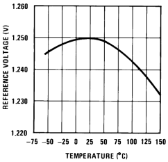
LM317A 906341.gif
Figure 7. Temperature Stability
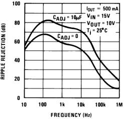
LM317A 906343.gif
Figure 9. Ripple Rejection
LM317A 906345.gif
Figure 11. Ripple Rejection
LM317A 906347.gif
Figure 13. Line Transient Response
LM317A 906338.gif
Figure 2. Current Limit
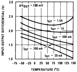
LM317A 906340.gif
Figure 4. Dropout Voltage
LM317A 906368.gif
Figure 6. VOUT vs VIN, VOUT = 5V
LM317A 906342.gif
Figure 8. Minimum Operating Current
LM317A 906344.gif
Figure 10. Ripple Rejection
LM317A 906346.gif
Figure 12. Output Impedance
LM317A 906348.gif
Figure 14. Load Transient Response