SNVS782C October 2010 – August 2015 LM3243
PRODUCTION DATA.
- 1 Features
- 2 Applications
- 3 Description
- 4 Revision History
- 5 Pin Configuration and Functions
- 6 Specifications
- 7 Detailed Description
- 8 Application and Implementation
- 9 Power Supply Recommendations
- 10Layout
- 11Device and Documentation Support
- 12Mechanical, Packaging, and Orderable Information
Package Options
Mechanical Data (Package|Pins)
- YFQ|16
Thermal pad, mechanical data (Package|Pins)
Orderable Information
6 Specifications
6.1 Absolute Maximum Ratings
over operating free-air temperature range (unless otherwise noted)(1)(2)(3)| MIN | MAX | UNIT | ||
|---|---|---|---|---|
| VDD, PVIN to SGND | −0.2 | 6 | V | |
| PGND to SGND | −0.2 | 0.2 | V | |
| EN, FB, VCON, BP, MODE | (SGND − 0.2) | (VDD + 0.2) | V | |
| SW, ACB | (PGND − 0.2) | (PVIN + 0.2) | V | |
| PVIN to VDD | −0.2 | 0.2 | V | |
| Continuous power dissipation(4) | Internally limited | |||
| Junction temperature, TJ-MAX | 150 | °C | ||
| Maximum lead temperature (soldering, 10 sec) | 150 | °C | ||
| Storage temperature, Tstg | −65° | 150 | °C | |
(1) Stresses beyond those listed under Absolute Maximum Ratings may cause permanent damage to the device. These are stress ratings only, which do not imply functional operation of the device at these or any other conditions beyond those indicated under Recommended Operating Conditions. Exposure to absolute-maximum-rated conditions for extended periods may affect device reliability.
(2) Absolute Maximum Ratings indicate limits beyond which damage to the component may occur. Recommended Operating Conditions are conditions under which operation of the device is specified. Operating Ratings do not imply verified performance limits. For performance limits and associated test conditions, see Electrical Characteristics.
(3) All voltages are with respect to the potential at the GND pins. The LM3243 is designed for mobile phone applications where turnon after power-up is controlled by the system controller and where requirements for a small package size overrule increased die size for internal undervoltage lock-out (UVLO) circuitry. Thus, it should be kept in shutdown by holding the EN pin LOW until the input voltage exceeds 2.7 V.
(4) Internal thermal shutdown circuitry protects the device from permanent damage. Thermal shutdown engages at TJ = 150°C (typical) and disengages at TJ = 130°C (typical).
6.2 ESD Ratings
| VALUE | UNIT | |||
|---|---|---|---|---|
| V(ESD) | Electrostatic discharge | Human-body model (HBM), per ANSI/ESDA/JEDEC JS-001(1) | ±2000 | V |
(1) JEDEC document JEP155 states that 500-V HBM allows safe manufacturing with a standard ESD control process.
6.3 Recommended Operating Conditions
over operating free-air temperature range (unless otherwise noted)(1)(2)| MIN | NOM | MAX | UNIT | ||
|---|---|---|---|---|---|
| Input voltage | 2.7 | 5.5 | V | ||
| Recommended load current | 2.5 | A | |||
| Junction temperature, TJ | −30 | 125 | °C | ||
| Ambient temperature, TA(3) | −30 | 90 | °C | ||
(1) Stresses beyond those listed under Absolute Maximum Ratings may cause permanent damage to the device. These are stress ratings only, which do not imply functional operation of the device at these or any other conditions beyond those indicated under Recommended Operating Conditions. Exposure to absolute-maximum-rated conditions for extended periods may affect device reliability.
(2) All voltages are with respect to the potential at the GND pins. The LM3243 is designed for mobile phone applications where turnon after power up is controlled by the system controller and where requirements for a small package size overrule increased die size for internal undervoltage lock-out (UVLO) circuitry. Thus, it should be kept in shutdown by holding the EN pin LOW until the input voltage exceeds 2.7 V.
(3) In applications where high-power dissipation and/or poor package thermal resistance is present, the maximum ambient temperature may have to be de-rated. Maximum ambient temperature (TA-MAX) is dependent on the maximum operating junction temperature (TJ-MAX-OP = 125°C), the maximum power dissipation of the device in the application (PD-MAX), and the junction-to ambient thermal resistance of the part/package in the application (RθJA), as given by the following equation: TA-MAX = TJ-MAX-OP – (RθJA × PD-MAX). At higher power levels duty cycle usage is assumed to drop (that is, max power 12.5% usage is assumed) for 2G mode.
6.4 Thermal Information
| THERMAL METRIC(1) | LM3243 | UNIT | |
|---|---|---|---|
| TMD (DSBGA) | |||
| 16 PINS | |||
| RθJA | Junction-to-ambient thermal resistance | 50 | °C/W |
(1) For more information about traditional and new thermal metrics, see the Semiconductor and IC Package Thermal Metrics application report, SPRA953.
6.5 Electrical Characteristics
Unless otherwise noted, all specifications apply to Typical System Application Diagram with: PVIN = VDD = EN = 3.8 V,BP = 0 V. All typical (TYP) limits apply for TA = TJ = 25°C, and all minimum (MIN) and maximum (MAX) apply over the full operating ambient temperature range (−30°C ≤ TA = TJ ≤ +90°C), unless otherwise specified.(1)(2)(3)
| PARAMETER | TEST CONDITIONS | MIN | TYP | MAX | UNIT | |
|---|---|---|---|---|---|---|
| VFB, LOW | Feedback voltage at low setting | VCON = 0.16 V, MODE = LOW(3) | 0.35 | 0.40 | 0.45 | V |
| VFB, HIGH | Feedback voltage at high setting | VCON = 1.44 V, VIN = 3.9 V, MODE = LOW(3) |
3.492 | 3.6 | 3.708 | V |
| ISHDN | Shutdown supply current | EN = SW = VCON = 0 V(4) | 0.02 | 4 | µA | |
| Iq_PFM | DC bias current into VDD | No switching(5)
MODE = HIGH |
260 | 310 | µA | |
| Iq_PWM | DC bias current into VDD | No switching(5)
MODE = LOW |
975 | 1100 | µA | |
| ILIM,PFET,Transient | Positive transient peak current limit | VCON = 0.6 V(6) | 1.9 | 2.1 | A | |
| ILIM,PFET,Steady State | Positive steady-state peak current limit | VACB = 3.05 V VCON = 0.6 V(6) |
1.34 | 1.45 | 1.65 | A |
| ILIM, P_ACB | Positive active current assist peak current limit | VCON = 0.6 V, VACB = 2.8 V(6) | 1.4 | 1.7 | 2 | A |
| ILIM, NFET | NFET switch negative peak current limit | VCON = 1 V(6) | −1.69 | −1.50 | −1.31 | A |
| FOSC | Average Internal oscillator frequency | VCON = 1 V | 2.43 | 2.7 | 2.97 | MHz |
| VIH | Logic HIGH input threshold | BP, EN, MODE | 1.2 | V | ||
| VIL | Logic LOW input threshold | BP, EN, MODE | 0.5 | V | ||
| IEN | EN pin pulldown current | EN = 3.6 V | 0 | 5 | 10 | µA |
| IIN | Pin input current | BP, MODE | –1 | 1 | µA | |
| IVCON | VCON pin leakage current | VCON = 1 V | –1 | 1 | µA | |
| Gain | VCON to VOUT Gain | 0.16 V ≤ VCON ≤ 1.44 V(7) | 2.5 | V/V | ||
(1) All voltages are with respect to the potential at the GND pins. The LM3243 is designed for mobile phone applications where turnon after power up is controlled by the system controller and where requirements for a small package size overrule increased die size for internal undervoltage lock-out (UVLO) circuitry. Thus, it should be kept in shutdown by holding the EN pin LOW until the input voltage exceeds 2.7 V.
(2) Minimum and Maximum limits are specified by design, test, or statistical analysis.
(3) The parameters in the electrical characteristics table are tested under open loop conditions at PVIN = VDD = 3.8 V. For performance over the input voltage range and closed-loop results, refer to the datasheet curves.
(4) Shutdown current includes leakage current of PFET.
(5) Iq specified here is when the part is not switching. For operating input current at no load, refer to datasheet curves.
(6) Current limit is built-in, fixed, and not adjustable.
(7) Linearity limits are ±3% or ±50 mV, whichever is larger.
6.6 System Characteristics
The following spec table entries are specified by design and verifications providing the component values in the Typical System Application Diagram are used (L = 1.5 µH, DCR = 120 mΩ, TOKO DFE201610C-1R5N, CIN = 10 µF, 6.3 V, 0402, Samsung CL05A106MQ5NUN, COUT = 10 µF + 4.7 µF + 3 × 1 µF + 3300 pF: 6.3 V, 0402, Samsung CL05A106MQ5NUN, CL05A475MQNRN; 6.3 V, 0201 Samsung CL03A105MQ3CSN; 6.3 V, 01005 Murata GRM022R60J332K). These parameters are not verified by production testing. Minimum (MIN) and maximum (MAX) values are specified over the ambient temperature range TA = −30°C to 90°C. Typical (TYP) values are specified at PVIN = VDD = EN = 3.8 V, BP = 0 V and TA = 25°C unless otherwise stated.| PARAMETER | TEST CONDITIONS | MIN | TYP | MAX | UNIT | |
|---|---|---|---|---|---|---|
| Rtot_drop | Total dropout resistance in bypass mode | VCON = 1.5 V Max value at VIN = 3.1 V Inductor ESR ≤ 151 mΩ |
45 | 55 | mΩ | |
| CIN | Pin input capacitance for BP, EN, MODE | Test frequency = 100 KHz | 5 | pF | ||
| IOUT | Maximum load current in PWM mode | Switcher + ACB | 2.5 | A | ||
| IOUT, PU | Maximum output transient pullup current limit | Switcher + ACB(1) | 3 | |||
| IOUT, PD, PWM | PWM maximum output transient pulldown current limit | −3 | ||||
| IOUT, MAX-PFM | Maximum output load current in PFM mode | VIN = 3.8 V, VCON < 1 MODE = HIGH(1) |
85 | mA | ||
| Linearity | Linearity in control range of VCON = 0.16 V to 1.44 V |
VIN = 4.2 V(2)
Monotonic in nature |
−3% | 3% | ||
| −50 | 50 | mV | ||||
| η | Efficiency | VIN = 3.8 V, VOUT = 1.8 V IOUT = 10 mA MODE = HIGH (PFM) |
79% | 82% | ||
| VIN = 3.8 V, VOUT = 0.5 V IOUT = 5 mA MODE = HIGH (PFM) |
58% | 60% | ||||
| VIN = 3.8 V, VOUT = 3.5 V IOUT = 1900 mA MODE = LOW (PWM) |
89% | 92% | ||||
| VIN = 3.8 V, VOUT = 2.5 V IOUT = 250 mA MODE = LOW (PWM) |
90% | 93% | ||||
| VIN = 3.8 V, VOUT = 1.6 V IOUT = 130 mA MODE = LOW (PWM) |
83% | 86% | ||||
| VIN = 3.8 V, VOUT = 1 V IOUT = 400 mA MODE = LOW (PWM) |
81% | 84% | ||||
| VRIPPLE | Ripple voltage at no pulse skipping condition | VIN = 0.4 V to 3.6 V VOUT = 0.4 V to 3.6 V, ROUT = 1.9 Ω(3) MODE = LOW |
1 | 3 | mVpp | |
| Ripple voltage at pulse skipping condition | VIN = 5.5 V to dropout, VOUT = 3.6 V, ROUT = 1.9 Ω(3) | 8 | ||||
| PFM ripple voltage | VIN = 3.2 V, VOUT < 1.125 V IOUT =10 mA, MODE = HIGH |
50 | ||||
| VIN = 3.2 V, VOUT ≤ 0.5 V, IOUT = 5 mA MODE = HIGH |
50 | |||||
| Line_tr | Line transient response | VIN = 3.6 V to 4.2 V, TR = TF = 10 µs, VOUT = 1 V IOUT = 600 mA, MODE = LOW |
50 | mVpk | ||
| Load_tr | Load transient response | VOUT = 3 V, TR = TF = 10 µs IOUT = 0 A to 1.2 A MODE = LOW |
40 | mVpk | ||
| Maximum Duty Cycle | Maximum duty cycle | MODE = LOW | 100% | |||
| PFM_Freq | Minimum PFM frequency | VIN = 3.2 V, VOUT = 1 V IOUT = 10 mA, MODE = HIGH |
100 | 160 | kHz | |
| VIN = 3.2 V, VOUT = 0.5 V IOUT = 5 mA, MODE = HIGH |
34 | 55 | ||||
(1) Current limit is built-in, fixed, and not adjustable.
(2) Linearity limits are ±3% or ±50 mV, whichever is larger.
(3) Ripple voltage should be measured at COUT electrode on a well-designed PC board and using the suggested inductor and capacitors.
6.7 Timing Requirements
| MIN | MAX | UNIT | ||
|---|---|---|---|---|
| tSETUP | Time for SW pin to become active upon power up; EN = LOW-to-HIGH | 30 | µs | |
| tON | Turnon time (time for output to reach 90% of final value after EN LOW-to-HIGH transition) EN = LOW-to-HIGH, VIN = 4.2 V, VCON = 1.36 V, VOUT = 3.4 V, IOUT ≤ 1 mA |
50 | µs | |
| tRESPONSE | Time for VOUT to rise from 0 V to 3 V (90% or 2.7 V); VIN = 4.2 V, RLOAD = 6.8 Ω, VCON = 0 V to 1.2 V |
20 | µs | |
| Time for VOUT to fall from 3.6 V to 2.6 V (10% or 2.7 V) VIN = 4.2 V, RLOAD = 6.8 Ω, VCON = 1.44 V to 1.04 V |
20 | |||
| Time for VOUT to rise from 1.8 V to 2.8 V (90% or 2.7 V) VIN = 4.2 V, RLOAD = 1.9 Ω, VCON = 0.72 V to 1.12 V |
15 | |||
| Time for VOUT to fall from 2.8 V to 1.8 V (10% or 1.9 V) VIN = 4.2 V, RLOAD = 1.9 Ω, VCON = 1.12 V to 0.72 V |
15 | |||
| Time for VOUT to rise from 0 V to 3.4 V (90% or 3.1 V) VIN = 4.2 V, RLOAD = 1.9 Ω, VCON = 0 V to 1.36 V |
20 | |||
| Time for VOUT to fall from 3.4 V to 0.4 V (10% or 0.7 V) VIN = 4.2 V, RLOAD = 1.9 Ω, VCON = 1.36 V to 0.16 V |
20 | |||
| tBypass | Time for VOUT to rise from 0 V to PVIN after BP LOW-to-HIGH transition (90%) VCON = 0 V, IOUT ≤ 1 mA |
20 | µs | |
| tBypass, ON | Bypass turnon time. Time for VOUT to rise from 0 V to PVIN after EN LOW-to-HIGH transition (90% or 3.24) EN = VIN= 3.8 V, IOUT ≤ 1 mA |
50 | µs | |
6.8 Typical Characteristics
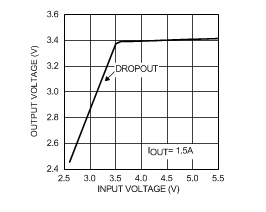
| VOUT = 3.4 V | VIN = 4.3 V down to Dropout | |
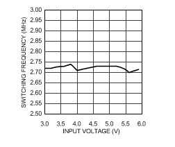
| VIN = 3.8 V | VOUT = 2.5 V | IOUT = 700 mA |
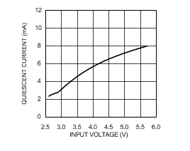
| 2.7 V < VIN< 5.5 V (No Load) | VOUT = 2.5 V | |
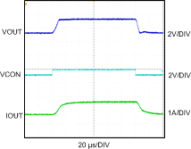
| VIN = 4.2 V | RLOAD = 1.9 Ω | VOUT = 1.4 V to 3.4 V |
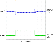
| VIN = 3.8 V | VOUT = 2.5 V | IOUT = 0 mA to 300 mA |
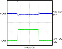
| VIN = 4.2 V | VOUT = 3 V | IOUT = 0 mA to 1.2 A |
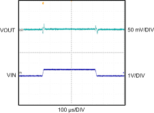
| VIN = 3.6 V to 4.2 V | RLOAD = 6.8 Ω | VOUT = 1 V |
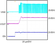
| VIN = 4.2 V | VOUT = 3.4 V | No load, EN = Low-to-High |
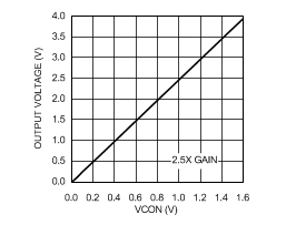
| VIN = 4.2 V | RLOAD = 6.8 Ω | 0.16 V < VCON < 1.4 V |
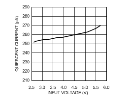
| 2.7 V < VIN< 5.5 V (No Load) | VOUT = 1 V | |
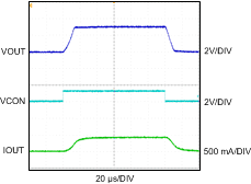
| VIN = 3.8 V | RLOAD = 6.8 Ω | VOUT = 0 V to 3 V |
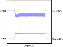
| VIN = 3.6 V | VOUT = 1 V | IOUT = 0 mA to 60 mA |
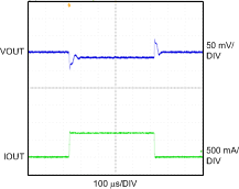
| VIN = 3.8 V | VOUT = 3 V | IOUT = 0 mA to 700 mA |
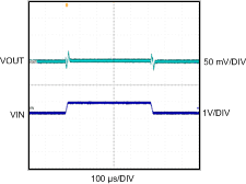
| VIN = 3.6 V to 4.2 V | RLOAD = 6.8 Ω | VOUT = 2.5 V |
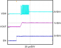
| VIN = 3.8 V | VOUT = 1 V | No load, EN = Low-to-High |
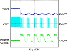
| VIN = 4.2 V | RLOAD = 6.8 Ω to VOUT Shorted | VOUT = 2.5 V |