SNVS875O August 2012 – December 2015 LM3262
PRODUCTION DATA.
- 1 Features
- 2 Applications
- 3 Description
- 4 Revision History
- 5 Pin Configuration and Functions
- 6 Specifications
- 7 Detailed Description
- 8 Application and Implementation
- 9 Power Supply Recommendations
- 10Layout
- 11Device and Documentation Support
- 12Mechanical, Packaging, and Orderable Information
Package Options
Mechanical Data (Package|Pins)
- YFQ|9
Thermal pad, mechanical data (Package|Pins)
Orderable Information
1 Features
- Operates from a Single Li-Ion Cell (2.5 V to 5.5 V)
- 6-MHz (Typical) PWM Switching Frequency
- Adjustable Output Voltage (0.4 V to 3.6 V)
- 800-mA Maximum Load Capability (up to 1 A in Bypass Mode)
- High Efficiency (93% Typical at 3.8 VIN, 3.4 VOUT at 500 mA)
- Automatic ECO/PWM/BP Mode Change
- Current and Thermal Overload Protection
- Multi-Function VCON Pin
(Eliminates Need for Separate BPEN Control) - Soft-Start Function
- Small Chip Inductor in 0805 (2012) Case Size
- 25-µA (Typical) IQ in Sleep Mode
- 5-µs (Typical) Rise Time and Fall Time for
2-V Step - 9-Pin DSBGA Package
2 Applications
- HSUPA, LTE Cellular Phones
- TD-SCDMA and TD-LTE
- Hand-Held Radios
- RF PC Cards
- Battery-Powered RF Devices
- USB-Powered Portable Applications
3 Description
The LM3262 is a DC-DC converter optimized for powering RF power amplifiers (PAs) from a single lithium-ion cell; however, it may be used in many other applications such as USB-powered portable applications. The device 2.5-V to 5.5-V input voltage can be stepped down to an adjustable output voltage range from 0.4 V to 3.6 V. Output voltage is set using a VCON analog input which enables improved RF-stage PA efficiencies.
The LM3262 offers five modes of operation. In pulse width modulation (PWM) mode the device operates at a fixed frequency of 6 MHz (typical), which minimizes RF interference at medium-to-low loads. At light load, the device enters into ECO mode automatically and operates with reduced switching frequency. In ECO mode, the quiescent current is reduced and extends the battery life. Shutdown mode turns the device off and reduces battery consumption to 0.1 µA (typical). At low-battery condition, bypass mode reduces the voltage dropout to less than 50 mV (typical). The device also features a sleep mode.
The LM3262 is available in a 9-pin, lead-free DSBGA package. A high-switching frequency (6 MHz) allows use of only three tiny surface-mount components: one inductor and two ceramic capacitors.
Device Information(1)
| PART NUMBER | PACKAGE | BODY SIZE (MAX) |
|---|---|---|
| LM3262 | DSGBA (9) | 1.51 mm × 1.385 mm |
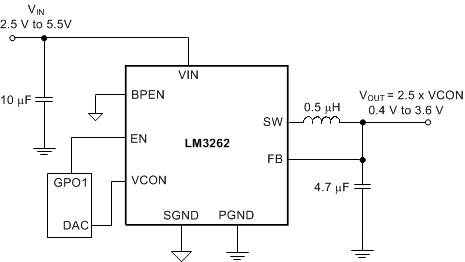
Typical Application Circuit
