SNVS837B June 2013 – April 2016 LM3263
PRODUCTION DATA.
- 1 Features
- 2 Applications
- 3 Description
- 4 Revision History
- 5 Pin Configuration and Functions
- 6 Specifications
-
7 Detailed Description
- 7.1 Overview
- 7.2 Functional Block Diagram
- 7.3
Feature Description
- 7.3.1 PWM Operation
- 7.3.2 PFM Operation
- 7.3.3 Active Current Assist and Analog Bypass (ACB)
- 7.3.4 Bypass Operation
- 7.3.5 Dynamic Adjustment of Output Voltage
- 7.3.6 DC-DC Operating Mode Selection
- 7.3.7 Internal Synchronous Rectification
- 7.3.8 Current Limit
- 7.3.9 Timed Current Limit
- 7.3.10 Thermal Overload Protection
- 7.3.11 Start-Up
- 7.4 Device Functional Modes
- 7.5 Programming
- 7.6 Register Map
- 8 Application Information
- 9 Power Supply Recommendations
- 10Layout Considerations
- 11Device and Documentation Support
- 12Mechanical, Packaging, and Orderable Information
Package Options
Mechanical Data (Package|Pins)
- YFQ|16
Thermal pad, mechanical data (Package|Pins)
Orderable Information
8 Application Information
NOTE
Information in the following applications sections is not part of the TI component specification, and TI does not warrant its accuracy or completeness. TI’s customers are responsible for determining suitability of components for their purposes. Customers should validate and test their design implementation to confirm system functionality.
8.1 Application Information
The LM3262 DC-DC converter steps down an input voltage from 2.7 V to 5.5 V to a dynamically adjustable output voltage of 0.4 V to 3.6 V.
8.2 Typical Application
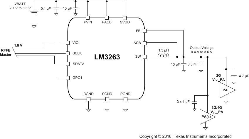
 Figure 27. LM3263 Typical Application
8.2.1 Design Requirements
For typical DC-DC converter applications use the parameters listed in Table 2.
Table 2. Design Parameters
| DESIGN PARAMETER | EXAMPLE VALUE |
|---|---|
| Input voltage range | 2.7 V to 5.5 V |
| Output voltage range | 0.4 V to 3.6 V |
| Output current | 1 A |
| Minimum effective output capacitance (including effects of AC bias, DC bias, temperature) | 10 µF |
8.2.2 Detailed Design Procedure
8.2.2.1 Recommended External Components
8.2.2.1.1 Inductor Selection
A 1.5-µH inductor is needed for optimum performance and functionality of the LM3263. In the case of 2G transmission current bursts, the effective overall RMS current requirements are reduced. Therefore, consult with the inductor manufacturers to determine if some of their smaller components are suitable even if the inductor specification does not appear to meet the LM3263 RMS current specifications.
The LM3263 automatically manages the inductor peak and RMS current (or steady-state current peak) through the SW pin. The SW pin has two positive current limits. The first is the 1.45-A typical (or 1.65-A maximum) overcurrent protection. It sets the upper steady-state inductor peak current (as detailed in Electrical Characteristics ILIM,PFET,SteadyState). It is the dominant factor limiting the inductors ISAT requirement. The second is an over-limit current protection. It limits the maximum peak inductor current during large signal transients (for example, < 20 µs) to 1.9 A typical (or 2.1 A maximum). A minimum inductance of 0.3 µH must be maintained at the second current limit.
The ACB circuit automatically adjusts its output current to keep the steady-state inductor current below the steady-state peak current limit. Thus, the inductor RMS current is always effectively than the ILIM,PFET,SteadyState during the transmit burst. In addition, as in the case with 2G where the output current comes in bursts, the effective overall RMS current would be much lower.
For good efficiency, resistance of the inductor must be less than 0.2 Ω; TI recommends low-DCR inductors (< 0.2 Ω). Table 3 suggests some inductors and their suppliers.
Table 3. Suggested Inductors And Their Suppliers
| MODEL | VENDOR | DIMENSIONS | ISAT
(30% DROP IN INDUCTANCE) |
DCR |
|---|---|---|---|---|
| DFE201610C1R5N (1285AS-H-1R5M) |
TOKO | 2 mm × 1.6 mm × 1 mm | 2.2 A | 120 mΩ |
| LQM2MPN1R5MGH | Murata | 2 mm × 1.6 mm × 1 mm | 2 A | 104 mΩ |
| MAKK2016T1R5M | Taiyo-Yuden | 2 mm × 1.6 mm × 1 mm | 1.9 A | 115 mΩ |
| VLS201610MT-1R5N | TDK | 2 mm × 1.6 mm × 1 mm | 1.4 A | 151 mΩ |
| LQM21PN1R5MGH | Murata | 2 mm × 1.25 mm × 1 mm | 1.2 A | 110 mΩ |
8.2.2.1.2 Capacitor Selection
The LM3263 is designed to use ceramic capacitors for its input and output filters. Use a 10-µF capacitor for the input and approximately 10 µF actual total output capacitance. Capacitor types such as X5R, X7R are recommended for both filters. These provide an optimal balance between small size, cost, reliability, and performance for cell phones and similar applications. Table 4 lists suggested part numbers and suppliers. DC bias characteristics of the capacitors must be considered while selecting the voltage rating and case size of the capacitor. Smaller case sizes for the output capacitor mitigate piezo-electric vibrations of the capacitor when the output voltage is stepped up and down at fast rates. However, they have a bigger percentage drop in value with dc bias. For even smaller total solution size, 0402 (1005) case size capacitors are recommended for filtering. Use of multiple 2.2-µF or 1-µF capacitors can also be considered. For RF PA applications, split the output capacitor between DC-DC converter and RF PAs; TI recomments 10 µF (COUT1) + 4.7 µF (COUT2) + 3 × 1 µF (COUT3)(assuming one 2G PA and three 3G/4G PAs — COUT2 is for 2G PA, and COUT3 is for 3G/4G PA). The optimum capacitance split is application dependent, and for stability the actual total capacitance (taking into account effects of capacitor DC bias, temperature de-rating, aging and other capacitor tolerances) must target 10 µF with 2.5-V DC bias (measured at 0.5 VRMS). Place all the output capacitors very close to the respective device. TI highly recommends placing a high-frequency capacitor (3300 pF) next to COUT1.
Table 4. Suggested Capacitors And Their Suppliers
| CAPACITANCE | MODEL | SIZE (W × L) | VENDOR |
|---|---|---|---|
| 10 µF | GRM185R60J106M | 1.6 mm × 0.8 mm | Murata |
| 10 µF | CL05A106MP5NUN | 1 mm × 0.5 mm | Samsung |
| 4.7 µF | CL05A475MP5NRN | 1 mm × 0.5 mm | Samsung |
| 1 µF | CL03A105MP3CSN | 0.6 mm × 0.3 mm | Samsung |
| 1 µF | C0603X5R0J105M | 0.6 mm × 0.3 mm | TDK |
| 3300 pF | GRM022R60J332K | 0.4 mm × 0.2 mm | Murata |
8.2.3 Application Curves

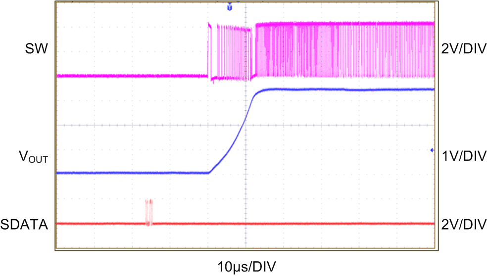
| VBATT = 4.2 V | VOUT = 3.4 V | No load |

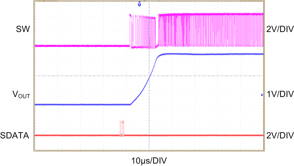
| VBATT = 4.2 V | VOUT = 3.4 V | No load |