SNVS793D November 2011 – May 2015 LM3269
PRODUCTION DATA.
- 1 Features
- 2 Applications
- 3 Description
- 4 Revision History
- 5 Pin Configuration and Functions
- 6 Specifications
- 7 Detailed Description
- 8 Application and Implementation
- 9 Power Supply Recommendations
- 10Layout
- 11Device and Documentation Support
- 12Mechanical, Packaging, and Orderable Information
Package Options
Mechanical Data (Package|Pins)
- YZR|12
Thermal pad, mechanical data (Package|Pins)
Orderable Information
1 Features
- Operates From a Single Li-Ion Cell: 2.7 V to 5.5 V
- Adjustable Output Voltage: 0.6 V to 4.2 V
- Automatic PFM or PWM Mode Change
- 750-mA Maximum Load Capability for
VBATT ≥ 3 V, VOUT = 3.8 V - 2.4-MHz (typical) Switching Frequency
- Seamless Buck-Boost Mode Transition
- Fast Output Voltage Transition: 1.4 V to 3 V
in 10 µs - High-Efficiency: 95% typical at VBATT = 3.7 V, VOUT = 3.3 V, at 300 mA
- Input Overcurrent Limit
- Internal Compensation
2 Applications
- Power Supply for 3G/4G Power Amplifiers
- Cellular Phones
- Portable Hard Disk Drives
- PDAs
3 Description
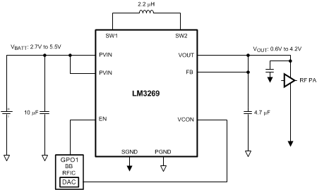
The LM3269 is buck-boost DC-DC converter designed to generate output voltages above or below a given input voltage and is particularly suitable for portable applications powered by a single-cell Li-ion battery.
The LM3269 operates at a 2.4-MHz typical switching frequency in full synchronous operation and provides seamless transitions between buck and boost operating regimes. The LM3269 operates in energy-saving Pulse Frequency Modulation (PFM) mode for increased efficiencies and current savings during low-power RF transmission modes.
The power converter topology needs only one inductor and two capacitors. A unique internal power switch topology enables high overall efficiency.
The LM3269 is internally compensated for buck and boost modes of operation, thus providing an optimal transient response.
When considering using the LM3269 in a system design, please review the layout instruactions at the end of this document.
Device Information(1)
| PART NUMBER | PACKAGE | BODY SIZE (MAX) |
|---|---|---|
| LM3269 | DSBGA (12) | 2.529 mm x 2.022 mm |
- For all available packages, see the orderable addendum at the end of the data sheet.
Typical Application
