SNVS793D November 2011 – May 2015 LM3269
PRODUCTION DATA.
- 1 Features
- 2 Applications
- 3 Description
- 4 Revision History
- 5 Pin Configuration and Functions
- 6 Specifications
- 7 Detailed Description
- 8 Application and Implementation
- 9 Power Supply Recommendations
- 10Layout
- 11Device and Documentation Support
- 12Mechanical, Packaging, and Orderable Information
Package Options
Mechanical Data (Package|Pins)
- YZR|12
Thermal pad, mechanical data (Package|Pins)
Orderable Information
10 Layout
10.1 Layout Guidelines
10.1.1 Overview
PC board layout is critical to successfully designing a DC-DC converter into a product. A properly planned board layout optimizes the performance of a DC-DC converter and minimizes effects on surrounding circuitry while also addressing manufacturing issues that can have adverse impact on board quality and final product yield.
10.1.1.1 PCB
Poor board layout can disrupt the performance of a DC-DC converter and surrounding circuitry by contributing to EMI, ground bounce, and resistive voltage loss in the traces. Erroneous signals could be sent to the DC-DC converter IC, resulting in poor regulation or instability. Poor layout can also result in re-flow problems leading to poor solder joints between the DSBGA package and board pads. Poor solder joints can result in erratic or degraded performance of the converter.
10.1.1.1.1 Energy Efficiency
Minimize resistive losses by using wide traces between the power components and doubling up traces on multiple layers when possible.
10.1.1.1.2 EMI
By its very nature, any switching converter generates electrical noise. The circuit board designer’s challenge is to minimize, contain, or attenuate such switcher-generated noise. A high-frequency switching converter, such as the LM3269, switches Ampere level currents within nanoseconds, and the traces interconnecting the associated components can act as radiating antennas. The following guidelines are offered to help to ensure that EMI is maintained within tolerable levels.
To help minimize radiated noise:
- Place the LM3269 switcher, its input capacitor, and output filter inductor and capacitor close together, and make the interconnecting traces as short as possible.
- Arrange the components so that the switching current loops curl in the same direction. During the first half of each cycle (buck mode), current flows from the input filter capacitor, through the internal PFET of the LM3269 and the inductor, to the output filter capacitor, then back through ground, forming a current loop. In the second half of each cycle (buck mode), current is pulled up from ground, through the internal synchronous NFET of the LM3269 by the inductor, to the output filter capacitor and then back through ground, forming a second current loop. Routing these loops so the current curls in the same direction prevents magnetic field reversal between the two half-cycles and reduces radiated noise.
- Make the current loop area(s) as small as possible.
To help minimize conducted noise in the ground-plane:
- Reduce the amount of switching current that circulates through the ground plane: Connect the ground bumps of the LM3269 and its input/output filter capacitors together using generous component-side copper fill as a pseudo-ground plane. Then connect this copper fill to the system ground-plane (if one is used) by multiple vias. These multiple vias help to minimize ground bounce at the LM3269 by giving it a low-impedance ground connection.
To help minimize coupling to the DC-DC converter's own voltage feedback trace:
- Route noise sensitive traces, such as the voltage feedback path (FB), as directly as possible from the switcher FB pad to the VOUT pad of the output capacitor, but keep it away from noisy traces between the power components. If possible, connect FB bump directly to VOUT bump.
To decouple common power supply lines, series impedances may be used to strategically isolate circuits:
- Take advantage of the inherent inductance of circuit traces to reduce coupling among function blocks, by way of the power supply traces.
- Use star connection for separately routing VBATT to PVIN and VBATT_PA (VCC1).
- Inserting a single ferrite bead in-line with a power supply trace may offer a favorable tradeoff in terms of board area, by allowing the use of fewer bypass capacitors.
10.1.1.2 Manufacturing Considerations
The LM3269 package employs a 12-bump (4 x 3) array of 300 micron solder balls, with a 0.5 mm pad pitch. A few simple design rules will go a long way toward ensuring a good layout.
- Pad size should be 0.265 ± 0.02 mm. Solder mask opening should be 0.375 ± 0.02 mm.
- As a thermal relief, connect to each pad with 9.5 mil wide, 5 mil long traces and incrementally increase each trace to its optimal width. Symmetry is important to ensure the solder bumps re-flow evenly. Refer to TI Application Note AN-1112 DSBGA Wafer Level Chip Scale Package (SNVA009).
10.1.1.3 LM3269 RF Evaluation Board
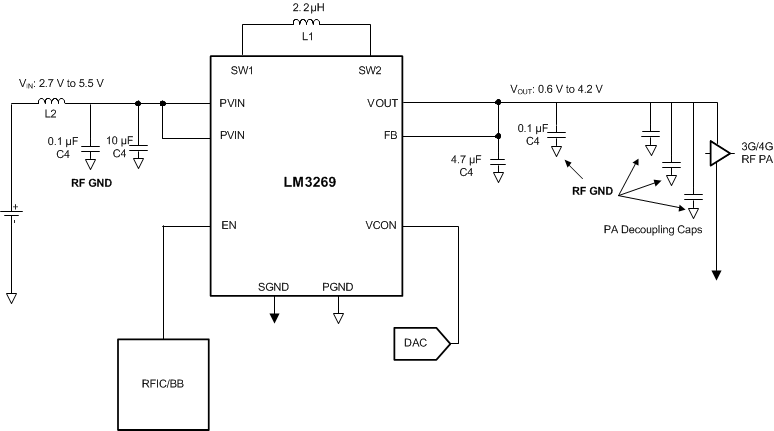 Figure 16. Simplified LM3269 RF Evaluation Board Schematic
- Input Capacitor C2 should be placed closer to LM3269 than C1.
- It is optional to add 100 nF (C1) on input of LM3269 for high frequency filtering.
- Bulk Output Capacitor C3 should be placed closer to LM3269 than C4.
- It is optional to add 100 nF (C4) on output of LM3269 for high frequency filtering.
- Connect both GND terminals of C1 and C4 directly to System RF GND layer of phone board.
- Connect bumps SGND (C2) directly to System GND.
- TI has seen improvement in high frequency filtering for small bypass capacitors (C1 and C4) when they are connected to System GND instead of same ground as PGND. These capacitors should be 0201 (0603 metric) case size for minimum footprint and best high frequency characteristics.
- A ferrite bead (L2) may help to improve high frequency noise.
Table 4. Recommended Components
| DESIGNATOR | PART NUMBER | VALUE | CASE SIZE | VENDOR |
|---|---|---|---|---|
| C1* | GMR033R60J104KE19D | 0.1 µF | 0201 (0603 metric) | Murata |
| C2 | C1608X5R0J106 | 10 µF | 0603 (1608 metric) | TDK |
| C3 | C1608X5RR0J475M | 4.7 µF | 0603 (1608 metric) | TDK |
| C4* | GRM033R60J104KE19D | 0.1 µF | 0201 (0603 metric) | Murata |
| L1 | MIPSZ2520D2R2 | 2.2 µH | 1008 (2520 metric) | FDK |
| L2* | BLM15AX100SN1 | 10 Ω | 0402 (1005 metric) | Murata |
| *Optional high frequency caps and high-frequency ferrit bead. | ||||
10.1.1.4 Component Placement
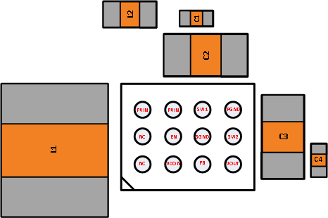 Figure 17. LM3269 Recommended Parts Placement (Top View)
10.1.1.5 PCB Considerations By Layer
10.1.1.5.1 VBATT
Use a star connection from VBATT to LM3269 and VBATT to PA VBATT (VCC1) connection. Do not daisy-chain VBATT connection to LM3269 circuit and then to PA device VBATT connection.
- Create a PGND island as shown. PGND pads of C2 (CIN) and C3 (COUT) must be isolated from each other. This PGND island will connect to the dedicated system ground with many vias.
- Each SW (C3) and (D2) bump will have a via in pad and an additional via next to it, to drop down the SW trace to layer
- SGND bump (C2) will have a via in pad, and directly connecting it to the system ground.
- FB (C1) should connect directly to the VOUT bump (D1).
- Have PVIN vias next to optional ferrite bead.
- Leave NC bumps (A1 and A2) floating; Do not connect to VBATT or GND
- VCON and Digital logic signals may be routed on this layer.
- VOUT (VCC2 of PA) can be routed on this layer.
- PVIN for the LM3269 can be routed on this layer.
- Each SW trace is routed on this layer. The width of each trace should be 15 mils (0.381 mm) for current capabilities. Have two vias bring each SW trace up to the inductor pads.
- Connect the PGND, SGND, and high Frequency vias from the top layer on this layer.
Top Layer (Numbers correspond to those in the Layout Examples section.)
Layer 2
Layer 3
Layer 4
10.2 Layout Examples
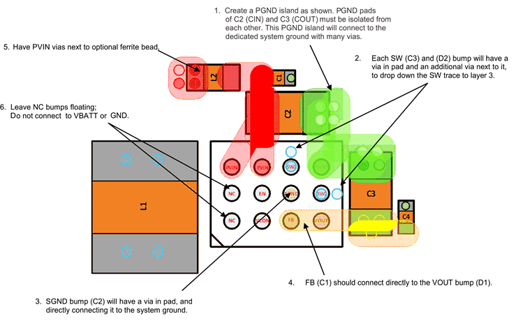 Figure 18. Top Layer
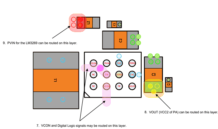 Figure 19. Board Layer 2 - Logic and PVIN Routing
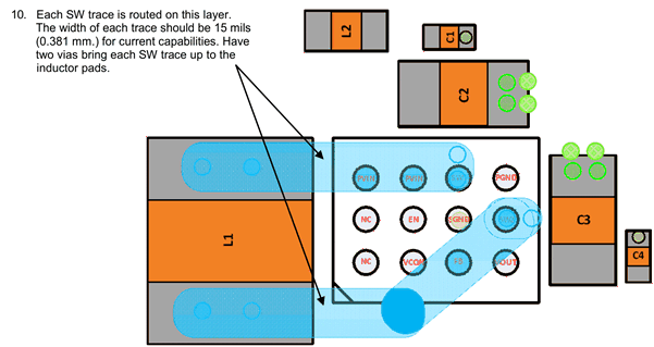 Figure 20. Board Layer 3 - SW Routing
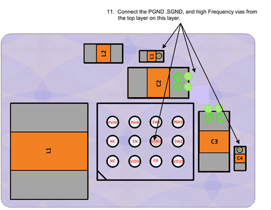 Figure 21. Board Layer 4 - System
10.3 DSBGA Package Assembly And Use
Use of the DSBGA package requires specialized board layout, precision mounting, and careful re-flow techniques, as detailed in Texas Instruments Application Note 1112. Refer to the section Surface Mount Technology (SMD) Assembly Considerations. For best results in assembly, alignment ordinals on the PC board should be used to facilitate placement of the device. The pad style used with DSBGA package must be the NSMD (non-solder mask defined) type. This means that the solder-mask opening is larger than the pad size. This prevents a lip that otherwise forms if the solder-mask and pad overlap from holding the device off the surface of the board and interfering with mounting. See Application Note AN-1112 DSBGA Wafer Level Chip Scale Package (SNVA009) for specific instructions how to do this.
The 12-bump package used for the LM3269 has 300 micron solder balls. The trace to each pad should enter the pad with a 90° entry angle to prevent debris from being caught in deep corners. Initially, the trace to each pad should be 9.5 mil wide, for a section approximately 5 mil long, as a thermal relief. Then each trance should neck up or down to its optimal width. The important criterion is symmetry. This ensures the solder bumps on the LM3269 re-flow evenly and that the device solders level to the board. In particular, special attention must be paid to the pads for bumps A3, B3, and D3. Because PVIN and PGND are typically connected to large copper planes, inadequate thermal relief can result in late or inadequate re-flow of these bumps.
The DSBGA package is optimized for the smallest possible size in applications with red or infrared opaque cases. Because the DSBGA package lacks the plastic encapsulation characteristic of larger devices, it is vulnerable to light. Backside metallization and/or epoxy coating, along with front-side shading by the printed circuit board, reduce this sensitivity. However, the package has exposed die edges. In particular, DSBGA devices are sensitive to light (in the red and infrared range) shining on the package's exposed die edges.