SNVS780E May 1998 – December 2016 LM337L
PRODUCTION DATA.
- 1 Features
- 2 Applications
- 3 Description
- 4 Revision History
- 5 Pin Configuration and Functions
- 6 Specifications
- 7 Detailed Description
- 8 Application and Implementation
- 9 Power Supply Recommendations
- 10Layout
- 11Device and Documentation Support
- 12Mechanical, Packaging, and Orderable Information
Package Options
Mechanical Data (Package|Pins)
- D|8
Thermal pad, mechanical data (Package|Pins)
Orderable Information
7 Detailed Description
7.1 Overview
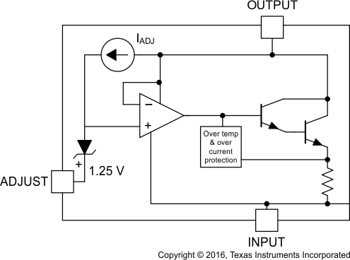
The LM337L devices are adjustable 3-terminal negative-voltage regulators capable of supplying 100 mA over an output voltage range of –1.2 V to –37 V. They are exceptionally easy to use, requiring only two external resistors to set the output voltage and one output capacitor for frequency compensation. In addition, LM337L offers full overload protection. Included on the chip are current limit, thermal overload protection and safe area protection. All overload protection circuitry remains fully functional even if the adjustment terminal is disconnected. The LMx37 devices serve a wide variety of applications, including local on-card regulation, programmable output-voltage regulation, and precision current regulation.
7.2 Functional Block Diagram

7.3 Feature Description
7.3.1 Output Voltage Adjustment
The Adjustment (ADJ) pin serves as a voltage adjustment reference for the output. The ADJ pin can be attached to a resistor divider circuit to adjust the output voltage level. The reference voltage VADJ will typically be 1.25 V higher than VO.
7.4 Device Functional Modes
7.4.1 Protection Diodes
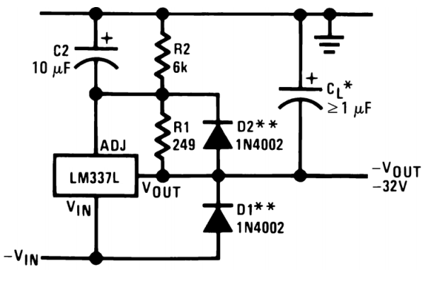
When external capacitors are used with any IC regulator, it is sometimes necessary to add protection diodes to prevent the capacitors from discharging through low current points into the regulator. Most 10-μF capacitors have low enough internal series resistance to deliver 20-A spikes when shorted. Although the surge is short, there is enough energy to damage parts of the IC. When an output capacitor is connected to a negative output regulator and the input is shorted, the output capacitor pulls current out of the output of the regulator. The current depends on the value of the capacitor, the output voltage of the regulator, and the rate at which VIN is shorted to ground. The bypass capacitor on the adjustment terminal can discharge through a low current junction. Discharge occurs when either the input, or the output, is shorted. Figure 15 shows the placement of the protection diodes.
