SNVS780E May 1998 – December 2016 LM337L
PRODUCTION DATA.
- 1 Features
- 2 Applications
- 3 Description
- 4 Revision History
- 5 Pin Configuration and Functions
- 6 Specifications
- 7 Detailed Description
- 8 Application and Implementation
- 9 Power Supply Recommendations
- 10Layout
- 11Device and Documentation Support
- 12Mechanical, Packaging, and Orderable Information
Package Options
Mechanical Data (Package|Pins)
- D|8
Thermal pad, mechanical data (Package|Pins)
Orderable Information
10 Layout
10.1 Layout Guidelines
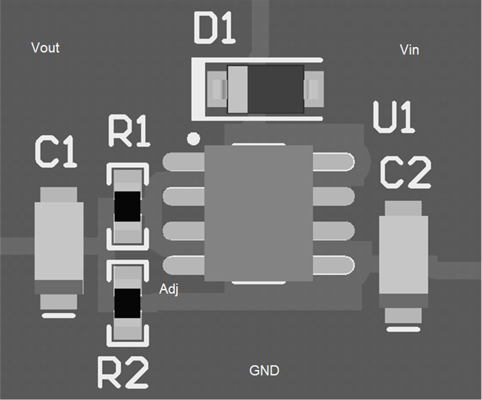
Some layout guidelines must be followed to ensure proper regulation of the output voltage with minimum noise. Traces carrying the load current must be wide to reduce the amount of parasitic trace inductance and the feedback loop from VOUT to ADJ must be kept as short as possible. To improve PSRR, a bypass capacitor can be placed at the ADJ pin and must be placed as close as possible to the IC. In cases when VIN shorts to ground, an external diode must be placed from VIN to VOUT to divert the surge current into the output capacitor and protect the IC. Similarly, in cases when a large bypass capacitor is placed at the ADJ pin and VOUT shorts to ground, an external diode must be placed from VOUT to ADJ to provide a path for the bypass capacitor to discharge. These diodes must be placed close to the corresponding IC pins to increase their effectiveness.
10.2 Layout Example
 Figure 9. LM337L Layout Example