SNOSDB3E June 2020 – November 2023 LM339LV-Q1 , LM393LV-Q1 , TL331LV-Q1 , TL391LV-Q1
PRODMIX
- 1
- 1 Features
- 2 Applications
- 3 Description
- 4 Pin Configuration and Functions
-
5 Specifications
- 5.1 Absolute Maximum Ratings
- 5.2 ESD Ratings
- 5.3 Recommended Operating Conditions
- 5.4 Thermal Information for TL3x1LV-Q1
- 5.5 Thermal Information, LM393LV-Q1
- 5.6 Thermal Information, LM339LV-Q1
- 5.7 Electrical Characteristics, TL3x1LV-Q1
- 5.8 Switching Characteristics, TL3x1LV-Q1
- 5.9 Electrical Characteristics, LM393LV-Q1
- 5.10 Switching Characteristics, LM393LV-Q1
- 5.11 Electrical Characteristics, LM339LV-Q1
- 5.12 Switching Characteristics, LM339LV-Q1
- 5.13 Typical Characteristics
- 6 Detailed Description
-
7 Application and Implementation
- 7.1 Application Information
- 7.2 Typical Applications
- 7.3 Power Supply Recommendations
- 7.4 Layout
- 8 Device and Documentation Support
- 9 Revision History
- 10Mechanical, Packaging, and Orderable Information
Package Options
Mechanical Data (Package|Pins)
Thermal pad, mechanical data (Package|Pins)
Orderable Information
7.1.2 Hysteresis
The basic comparator configuration may oscillate or produce a noisy "chatter" output if the applied differential input voltage is near the comparator's offset voltage. This usually occurs when the input signal is moving very slowly across the switching threshold of the comparator.
This problem can be prevented by the addition of hysteresis or positive feedback.
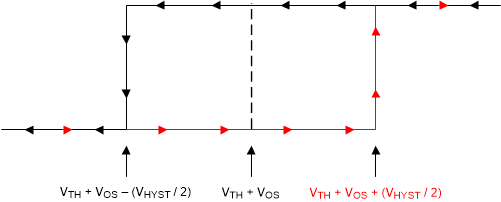
The hysteresis transfer curve is shown in Figure 7-2. This curve is a function of three components: VTH, VOS, and VHYST:
- VTH is the actual set voltage or threshold trip voltage.
- VOS is the internal offset voltage between VIN+ and VIN–. This voltage is added to VTH to form the actual trip point at which the comparator must respond to change output states.
- VHYST is the hysteresis (or trip window) that is designed to reduce comparator sensitivity to noise.
 Figure 7-2 Hysteresis Transfer Curve
For more information, please see Application Note SBOA219 "Comparator with and without hysteresis circuit".