SNOSDA4D June 2020 – November 2023 LM339LV , LM393LV , TL331LV , TL391LV
PRODMIX
- 1
- 1 Features
- 2 Applications
- 3 Description
- 4 Pin Configuration and Functions
-
5 Specifications
- 5.1 Absolute Maximum Ratings
- 5.2 ESD Ratings
- 5.3 Recommended Operating Conditions
- 5.4 Thermal Information for TL3x1LV
- 5.5 Thermal Information, LM393LV
- 5.6 Thermal Information, LM339LV
- 5.7 Electrical Characteristics, TL3x1LV
- 5.8 Switching Characteristics, TL3x1LV
- 5.9 Electrical Characteristics, LM393LV
- 5.10 Switching Characteristics, LM393LV
- 5.11 Electrical Characteristics, LM339LV
- 5.12 Switching Characteristics, LM339LV
- 5.13 Typical Characteristics
- 6 Detailed Description
-
7 Application and Implementation
- 7.1 Application Information
- 7.2 Typical Applications
- 7.3 Power Supply Recommendations
- 7.4 Layout
- 8 Device and Documentation Support
- 9 Revision History
- 10Mechanical, Packaging, and Orderable Information
Package Options
Mechanical Data (Package|Pins)
Thermal pad, mechanical data (Package|Pins)
- RTE|16
Orderable Information
5.13 Typical Characteristics
TA = 25°C, VS = 5 V, RPULLUP = 2.5k, CL = 15 pF, VCM = GND, VUNDERDRIVE = 100 mV, VOVERDRIVE = 100 mV unless otherwise noted.
 Figure 5-1 Supply Current vs. Supply Voltage
 Figure 5-3 Supply Current vs. Input Voltage, 1.8V
 Figure 5-5 Supply Current vs. Input Voltage, 5V
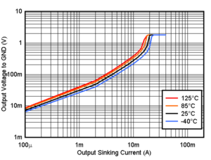 Figure 5-7 Output Sinking Current vs. Output Voltage, 1.8V
 Figure 5-9 Output Sinking Current vs. Output Voltage, 5V
 Figure 5-11 Risetime vs. Capacitive Load
 Figure 5-13 Propagation Delay, High to Low, 1.8V
 Figure 5-15 Propagation Delay, High to Low, 3.3V
 Figure 5-17 Propagation Delay, High to Low, 5V
 Figure 5-19 Offset Voltage vs. Input Votlage at 125°C, 1.8V
 Figure 5-21 Offset Voltage vs. Input Votlage at 25°C, 1.8V
 Figure 5-23 Offset Voltage vs. Input Votlage at -40°C, 1.8V
 Figure 5-25 Offset Voltage vs. Supply Voltage at 125°C, VIN=V+
 Figure 5-27 Offset Voltage vs. Supply Voltage at 25°C, VIN=V+
 Figure 5-29 Offset Voltage vs. Supply Voltage at -40°C, VIN=V+
 Figure 5-2 Supply Current vs. Temperature
 Figure 5-4 Supply Current vs. Input Voltage, 3.3V
 Figure 5-6 Input Bias Current vs. Temperature
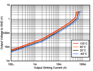 Figure 5-8 Output Sinking Current vs. Output Voltage, 3.3V
 Figure 5-10 Sinking Short Circuit Current vs. Temperature
 Figure 5-12 Falltime vs. Capacitive Load
 Figure 5-14 Propagation Delay, Low to High, 1.8V
 Figure 5-16 Propagation Delay, Low to High, 3.3V
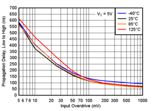 Figure 5-18 Propagation Delay, Low to High, 5V
 Figure 5-20 Offset Voltage vs. Input Votlage at 125°C, 5V
 Figure 5-22 Offset Voltage vs. Input Votlage at 25°C, 5V
 Figure 5-24 Offset Voltage vs. Input Votlage at -40°C, 5V
 Figure 5-26 Offset Voltage vs. Supply Voltage at 125°C, VIN=0V
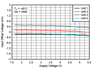 Figure 5-28 Offset Voltage vs. Supply Voltage at 25°C, VIN=0V
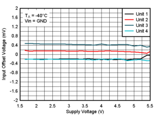 Figure 5-30 Offset Voltage vs. Supply Voltage at -40°C, VIN=0V