SNOSD64 June 2017 LM340-MIL
PRODUCTION DATA.
- 1 Features
- 2 Applications
- 3 Description
- 4 Revision History
- 5 Pin Configuration and Functions
- 6 Specifications
- 7 Detailed Description
- 8 Application and Implementation
- 9 Power Supply Recommendations
- 10Layout
- 11Device and Documentation Support
- 12Mechanical, Packaging, and Orderable Information
Package Options
Mechanical Data (Package|Pins)
- NDS|2
Thermal pad, mechanical data (Package|Pins)
Orderable Information
8 Application and Implementation
NOTE
Information in the following applications sections is not part of the TI component specification, and TI does not warrant its accuracy or completeness. TI’s customers are responsible for determining suitability of components for their purposes. Customers should validate and test their design implementation to confirm system functionality.
8.1 Application Information
The LM340-MIL device is designed with thermal protection, output short-circuit protection, and output transistor safe area protection. However, as with any IC regulator, it becomes necessary to take precautions to assure that the regulator is not inadvertently damaged. The following describes possible misapplications and methods to prevent damage to the regulator.
8.1.1 Shorting the Regulator Input
When using large capacitors at the output of these regulators, a protection diode connected input to output (Figure 15) may be required if the input is shorted to ground. Without the protection diode, an input short causes the input to rapidly approach ground potential, while the output remains near the initial VOUT because of the stored charge in the large output capacitor. The capacitor will then discharge through a large internal input to output diode and parasitic transistors. If the energy released by the capacitor is large enough, this diode, low current metal, and the regulator are destroyed. The fast diode in Figure 15 shunts most of the capacitors discharge current around the regulator. Generally no protection diode is required for values of output capacitance ≤ 10 μF.
8.1.2 Raising the Output Voltage Above the Input Voltage
Because the output of the device does not sink current, forcing the output high can cause damage to internal low current paths in a manner similar to that just described in Shorting the Regulator Input.
8.1.3 Regulator Floating Ground
When the ground pin alone becomes disconnected, the output approaches the unregulated input, causing possible damage to other circuits connected to VOUT. If ground is reconnected with power ON, damage may also occur to the regulator. This fault is most likely to occur when plugging in regulators or modules with on card regulators into powered up sockets. The power must be turned off first, the thermal limit ceases operating, or the ground must be connected first if power must be left on. See Figure 16.
8.1.4 Transient Voltages
If transients exceed the maximum rated input voltage of the device, or reach more than 0.8 V below ground and have sufficient energy, they will damage the regulator. The solution is to use a large input capacitor, a series input breakdown diode, a choke, a transient suppressor or a combination of these.
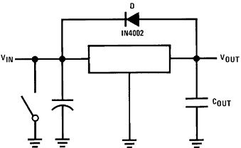 Figure 15. Input Short
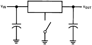 Figure 16. Regulator Floating Ground
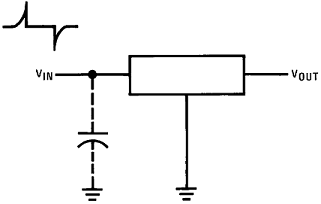 Figure 17. Transients
When a value for θ(H–A) is found, a heat sink must be selected that has a value that is less than or equal to this number.
θ(H–A) is specified numerically by the heat sink manufacturer in this catalog or shown in a curve that plots temperature rise vs power dissipation for the heat sink.
8.2 Typical Application
8.2.1 Fixed Output Voltage Regulator
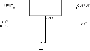
The LM340-MIL device is primarily designed to provide fixed output voltage regulation. Figure 18 shows the simplest implementation of the LM340-MIL device.
8.2.1.1 Design Requirements
The device component count is very minimal. Although not required, TI recommends employing bypass capacitors at the output for optimum stability and transient response. These capacitors must be placed as close as possible to the regulator. If the device is located more than 6 inches from the power supply filter, it is required to employ input capacitor.
8.2.1.2 Detailed Design Procedure
The output voltage is set based on the device variant. LM340-MIL device is available in 5-V, 12-V and 15-V regulator options.
8.2.1.3 Application Curve
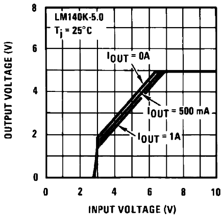
| VOUT = 5 V |
8.3 System Examples
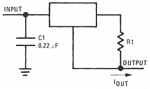
ΔIQ = 1.3 mA over line and load changes.
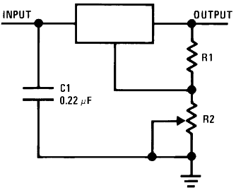
R2 5 V/R1 > 3 IQ, load regulation (Lr) ≈ [(R1 + R2)/R1]
(Lr of LM340-MIL-5).
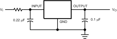 Figure 22. High Input Voltage Circuit With Series Resistor
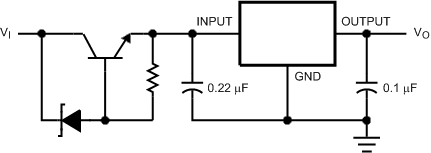 Figure 23. High Input Voltage Circuit implementation With Transistor
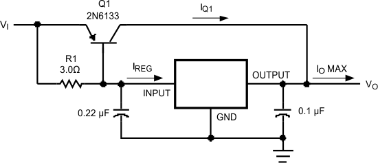
R1 = 0.9 / IREG = β(Q1) VBE(Q1) / IREG Max (β +1) – IO Max
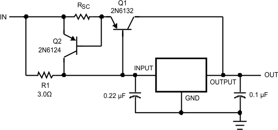
R1 = βVBE(Q1) / IREG Max (β +1) – IO Max
 Figure 26. Device Used With Negative Regulator LM79xx