SNOSD64
June 2017
LM340-MIL
PRODUCTION DATA.
1
Features
2
Applications
3
Description
4
Revision History
5
Pin Configuration and Functions
6
Specifications
6.1
Absolute Maximum Ratings
6.2
ESD Ratings
6.3
Recommended Operating Conditions
6.4
Thermal Information
6.5
Electrical Characteristics: VO = 5 V, VI = 10 V
6.6
Electrical Characteristics: VO = 12 V, VI = 19 V
6.7
Electrical Characteristics: VO = 15 V, VI = 23 V
6.8
Typical Characteristics
7
Detailed Description
7.1
Overview
7.2
Functional Block Diagram
7.3
Feature Description
7.3.1
Output Current
7.3.2
Current Limiting Feature
7.3.3
Thermal Shutdown
7.4
Device Functional Modes
8
Application and Implementation
8.1
Application Information
8.1.1
Shorting the Regulator Input
8.1.2
Raising the Output Voltage Above the Input Voltage
8.1.3
Regulator Floating Ground
8.1.4
Transient Voltages
8.2
Typical Application
8.2.1
Fixed Output Voltage Regulator
8.2.1.1
Design Requirements
8.2.1.2
Detailed Design Procedure
8.2.1.3
Application Curve
8.3
System Examples
9
Power Supply Recommendations
10
Layout
10.1
Layout Guidelines
10.2
Layout Example
10.3
Heat Sinking DDPAK/TO-263 and SOT-223 Package Parts
11
Device and Documentation Support
11.1
Documentation Support
11.1.1
Related Documentation
11.2
Receiving Notification of Documentation Updates
11.3
Community Resources
11.4
Trademarks
11.5
Electrostatic Discharge Caution
11.6
Glossary
12
Mechanical, Packaging, and Orderable Information
Package Options
Mechanical Data (Package|Pins)
NDS|2
MMSF012A
Thermal pad, mechanical data (Package|Pins)
Orderable Information
snosd64_oa
snosd64_pm
5
Pin Configuration and Functions
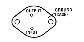
NDS Package
2-Pin TO-3
Top View
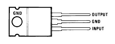
NDE Package
3-Pin TO-220
Top View
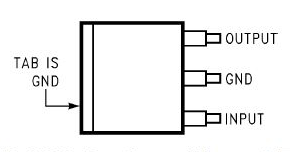
KTT Package
3-Pin DDPAK/TO-263
Top View
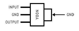
DCY Package
4-Pin SOT-223
Side View
Pin Functions
PIN
I/O
DESCRIPTION
NAME
NO.
INPUT
1
I
Input voltage pin
GND
2
I/O
Ground pin
OUTPUT
3
O
Output voltage pin