SNVS553C January 2008 – November 2016 LM3407
PRODUCTION DATA.
- 1 Features
- 2 Applications
- 3 Description
- 4 Revision History
- 5 Pin Configuration and Functions
- 6 Specifications
- 7 Detailed Description
- 8 Application and Implementation
- 9 Power Supply Recommendations
- 10Layout
- 11Device and Documentation Support
- 12Mechanical, Packaging, and Orderable Information
Package Options
Mechanical Data (Package|Pins)
- DGN|8
Thermal pad, mechanical data (Package|Pins)
- DGN|8
Orderable Information
8 Application and Implementation
NOTE
Information in the following applications sections is not part of the TI component specification, and TI does not warrant its accuracy or completeness. TI’s customers are responsible for determining suitability of components for their purposes. Customers should validate and test their design implementation to confirm system functionality.
8.1 Application Information
8.1.1 Switching Frequency Selection
The selection of switching frequency is based on the consideration of the conversion efficiency, size of the passive components, and the total solution cost. In general, increasing the switching frequency allows the use of smaller external components but decreases the conversion efficiency. Thus, the selection of switching frequency is a compromise between the system requirements and may vary from design to design. The LM3407 switching frequency can be set in the range from 300 kHz to 1 MHz by adjusting the value of RFS. The switching frequency is inversely proportional to the value of RFS. To ensure good operation stability, a resistor with 1% tolerance between 40 kΩ and 96 kΩ and with good thermal stability is suggested.
The switching frequency is estimated by Equation 2:

where
- fSW is the oscillator frequency
- RFS is the frequency setting resistance
Equation 2 is only valid for oscillator frequencies in the range of 300 kHz to 1 MHz, so the frequency setting resistance will be in the range of about 40 kΩ to 150 kΩ.
8.1.2 LED Current Setting
The LED current setting is important to the lifetime, reliability, and color temperature of the LED string. The LED current should be properly selected according to the characteristics of the LED used. Over-driving the LED array can cause the color temperature to shift and will shorten the lifetime of the LEDs. The output current of the LM3407 can be set by RISNS, which is calculated from Equation 3:

To ensure the accuracy of the output current, a resistor with 1% tolerance should be used for RISNS. It is also important for the designer to ensure that the rated power of the resistor is not exceeded with reasonable margin. For example, when IOUT is set to 350 mA, the total power dissipation on RISNS in steady state is (0.35 A)2 × 0.565 Ω, which equals 69 mW, indicating a resistor of 1/8W power rating is appropriate.
8.1.3 Input and Output Capacitors
The input capacitor supplies instantaneous current to the LM3407 converter when the internal power switch Q1 turns ON. The input capacitor filters the noise and transient voltage from the input power source. Using low ESR capacitors such as ceramic and tantalum capacitors is recommended. Similar to the selection criteria for the output capacitor, ceramic capacitors are the best choice for the input to the LM3407 due to their high ripple current rating, low ESR, and relatively small size compared to other types. A 4.7-µF X7R ceramic capacitor for the input capacitor is recommended
The output capacitor COUT is used to reduce LED current ripple, filter noise, and smooth output voltage. This capacitor should have low ESR and adequate capacitance. Excessively large output capacitances create long enable and disable times, which is particularly significant when a high dimming frequency is used. Because the loading and input conditions differ from design to design, a 2.2-µF X7R ceramic capacitor is a good initial selection. A DC voltage rating equal to or higher than twice the forward voltage of the LED string is recommended.
COUT is optional and can be omitted for applications where small brightness variation is acceptable. Omitting COUT also helps reduce the cost and board size of the converter. With the absence of COUT, the LED forward current equals the inductor current. To ensure proper operation of the converter, the peak inductor current must not exceed the rated forward current of the LEDs. Otherwise the LEDs may be damaged.
8.1.4 Selection of Inductor
To achieve accurate constant current output, the LM3407 is required to operate in Continuous Conduction Mode (CCM) under all operating conditions. In general, the magnitude of the inductor ripple current should be kept as small as possible. If the PCB size is not limited, higher inductance values result in better accuracy of the output current. However, to minimize the physical size of the circuit, an inductor with minimum physical outline should be selected such that the converter always operates in CCM and the peak inductor current does not exceed the saturation current limit of the inductor. The ripple and peak current of the inductor can be calculated as follows:
Inductor Peak to Peak Ripple Current:

Peak Inductor Current:

where
- n is the number of LEDs in a string
- VF is the forward voltage of one LED.
The minimum inductance required for the specific application can be calculated by Equation 6:

For applications with no output capacitor in place, the magnitude of the inductor ripple current should not be more than 20% of the average inductor current, which is equivalent to the output current, IOUT. However, in some situations the physical size of the required inductor may be too large and thus not allowed. The output capacitor can help absorb this current ripple to significantly reduce the ripple component along the LED string. With an output capacitor COUT in place, the magnitude of the inductor ripple current can be relaxed to 80% of the output current. Figure 23 illustrates the relationship between IOUT, IL(peak), and IL(ripple).
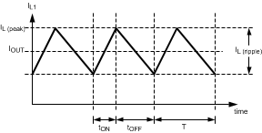 Figure 23. Relationship Between IOUT, IL(peak) and IL(ripple)
Table 1 provides the suggested inductance of the inductor for 500 kHz and 1 MHz switching frequency operation with COUT = 4.7 µF and IL(ripple) = 0.8 × IOUT
Table 1. Suggested Inductance Value of the Inductor
| VIN / V | Number of LED | ||||||
|---|---|---|---|---|---|---|---|
| 1 | 2 | 3 | 4 | 5 | 6 | 7 | |
| Inductor selection table for FSW = 500 kHz, COUT = 4.7 µF (1 µF for 1 LED) | |||||||
| 5 | 22 µH | ||||||
| 10 | 22 µH | 22 µH | |||||
| 15 | 22 µH | 22 µH | 22 µH | ||||
| 20 | 22 µH | 33 µH | 22 µH | 22 µH | 22 µH | ||
| 25 | 22 µH | 33 µH | 33 µH | 22 µH | 22 µH | 22 µH | |
| 30 | 22 µH | 47 µH | 33 µH | 33 µH | 33 µH | 22 µH | 22 µH |
| Inductor selection table for FSW = 1 MHz, COUT = 4.7 µF (1 µF for 1 LED) | |||||||
| 5 | 22 µH | ||||||
| 10 | 22 µH | 22 µH | |||||
| 15 | 22 µH | 22 µH | 22 µH | ||||
| 20 | 22 µH | 22 µH | 22 µH | 22 µH | 22 µH | ||
| 25 | 22 µH | 33 µH | 22 µH | 22 µH | 22 µH | 22 µH | |
| 30 | 22 µH | 33 µH | 33 µH | 33 µH | 22 µH | 22 µH | 22 µH |
8.1.5 Free-Wheeling Diode
The LM3407 is a non-synchronous floating buck converter that requires an external free-wheeling diode to provide a path for recirculating current from the inductor to the LED array when the power switch is turned OFF. Selecting the free-wheeling diode depends on both the output voltage and current. The diode must have a rated reverse voltage higher than the input voltage of the converter and a peak current rating higher than the expected maximum inductor current. Using a schottky diode with a low forward voltage drop can reduce power dissipation and enhance conversion efficiency.
8.2 Typical Applications
8.2.1 LM3407 Design Example
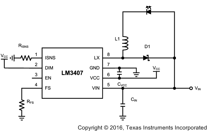 Figure 24. LM3407 Design Example Schematic
8.2.1.1 Design Requirements
- Input Voltage: VIN = 12 V ±10%
- LED String Voltage: VLED = 6.4 V (2 series white LEDs)
- LED Current: ILED = 350 mA
- Switching Frequency: fSW = 1 MHz
8.2.1.2 Detailed Design Procedure
This design is intended to be a small size, low-cost solution. An output capacitor will not be used to save on size and cost so a high switching frequency will be used and a higher value inductor than recommended in Table 1 will be used to keep LED current ripple lower.
8.2.1.2.1 Calculate RISNS
For 350 mA LED current calculate the value for RISNS using Equation 7.

Choose a standard value of RISNS = 0.565 Ω.
8.2.1.2.2 Calculate RFS
Calculate the value of RFS for 1-MHz switching frequency using Equation 8.

Choose a standard value of RFS = 40.2 kΩ.
8.2.1.2.3 Choose L
Referring to Table 1 the recommended inductor value for 12 V input and 2 LED output is 22 µH.
Choose a higher standard value of L = 33 µH to reduce ripple since an output capacitor will not be used for this design.
8.2.1.2.4 Choose CIN and CVCC
Choose the recommended values of CIN = 4.7 µF and CVCC = 1 µF. CIN should be a 16 V or greater ceramic capacitor and CVCC should be a 10 V or greater ceramic capacitor. Both should use an X5R or X7R dielectric.
8.2.1.3 Application Curve
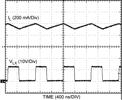 Figure 25. LED Current and Switch Voltage Waveforms
8.2.2 Typical Application for Driving 6 LEDs
Figure 26 shows a high voltage, 6-W application for driving 6 LEDs. The switching frequency is set at 1 MHz and the LED current is set at 350 mA.
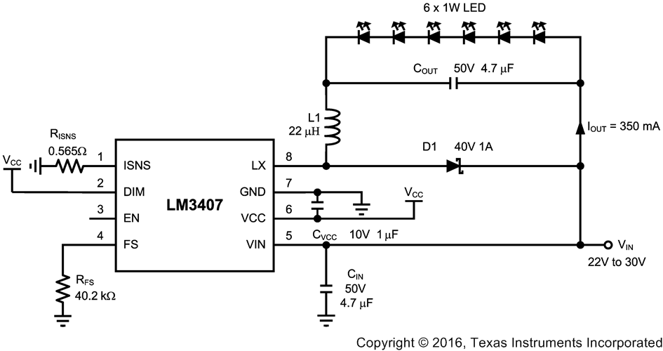 Figure 26. LM3407 6 LED Example Schematic
8.2.3 Typical Application for Driving 1 LED
Figure 27 shows a low voltage, 1-W application for driving 1 LED. The switching frequency is set at 1 MHz and the LED current is set at 350 mA.
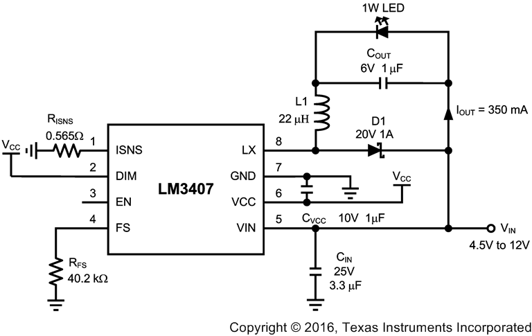 Figure 27. LM3407 1 LED Example Schematic