6 Specifications
6.1 Absolute Maximum Ratings
over operating free-air temperature range (unless otherwise noted)(1)
|
MIN |
MAX |
UNIT |
| VIN to GND |
–0.3 |
36 |
V |
| VIN to GND (transient) |
|
42 (500 ms) |
V |
| LX to GND |
–0.3 |
36 |
V |
| LX to GND (transient) |
–3 (2 ns) |
42 (500 ms) |
V |
| FS, ISNS, DIM, EN to GND |
–0.3 |
7 |
V |
| Storage temperature, Tstg |
–65 |
125 |
°C |
(1) Stresses beyond those listed under Absolute Maximum Ratings may cause permanent damage to the device. These are stress ratings only, which do not imply functional operation of the device at these or any other conditions beyond those indicated under Recommended Operating Conditions. Exposure to absolute-maximum-rated conditions for extended periods may affect device reliability.
6.2 ESD Ratings
|
VALUE |
UNIT |
| V(ESD) |
Electrostatic discharge |
Human-body model (HBM), per ANSI/ESDA/JEDEC JS-001(1) |
±2000 |
V |
| Charged-device model (CDM), per JEDEC specification JESD22-C101(2) |
±750 |
(1) JEDEC document JEP155 states that 500-V HBM allows safe manufacturing with a standard ESD control process.
(2) JEDEC document JEP157 states that 250-V CDM allows safe manufacturing with a standard ESD control process.
6.3 Recommended Operating Conditions
over operating free-air temperature range (unless otherwise noted)
|
MIN |
MAX |
UNIT |
| VIN |
4.5 |
30 |
V |
| Junction temperature |
–40 |
125 |
°C |
6.4 Thermal Information
| THERMAL METRIC(1) |
LM3407 |
UNIT |
| DGN (MSOP) |
| 8 PINS |
| RθJA |
Junction-to-ambient thermal resistance |
55.6 |
°C/W |
| RθJC(top) |
Junction-to-case (top) thermal resistance |
50.7 |
°C/W |
| RθJB |
Junction-to-board thermal resistance |
28.8 |
°C/W |
| ψJT |
Junction-to-top characterization parameter |
1.6 |
°C/W |
| ψJB |
Junction-to-board characterization parameter |
28.6 |
°C/W |
| RθJC(bot) |
Junction-to-case (bottom) thermal resistance |
4.9 |
°C/W |
6.5 Electrical Characteristics
MIN and MAX limits apply for TJ = –40°C to +125°C unless specified otherwise. VIN = 12 V unless otherwise indicated.
| PARAMETER |
TEST CONDITIONS |
MIN(1) |
TYP(2) |
MAX(1) |
UNIT |
| SYSTEM PARAMETERS |
| IIN |
Operating input current |
4.5 V ≤ VIN ≤ 30 V, LX = open,
VPWM = VEN = 5 V |
0.58 |
0.78 |
0.98 |
mA |
| IQ |
Quiescent Input current |
4.5 V ≤ VIN ≤ 30 V,
VPWM = 0 V, VEN = 5 V |
0.2 |
0.27 |
0.39 |
mA |
| ISHUT |
Shutdown input current |
VEN = 0 V |
36 |
48 |
60 |
µA |
| VUVLO |
Input undervoltage lockout threshold |
VIN Rising |
|
3.6 |
4.5 |
V |
| VUVLO-HYS |
UVLO hysteresis |
VIN Falling |
|
200 |
|
mV |
| VEN_H |
EN Pin HIGH threshold |
VEN Rising |
|
1.9 |
2.4 |
V |
| VEN_L |
EN Pin LOW threshold |
VEN Falling |
1.3 |
1.75 |
|
V |
| VDIM_H |
DIM Pin HIGH threshold |
VDIM Rising |
|
1.9 |
2.4 |
V |
| VDIM_L |
DIM Pin LOW threshold |
VDIM Falling |
1.3 |
1.75 |
|
V |
| fSW |
Switching frequency |
RT = 80 kΩ |
|
500 |
|
kHz |
| RT = 40 kΩ |
|
1000 |
|
| tON-MIN |
Minimum on-time |
|
|
200 |
|
ns |
| TSD |
Thermal shutdown threshold |
|
|
165 |
|
°C |
| TSD-HYS |
Thermal shutdown hysteresis |
|
|
25 |
|
| INTERNAL VOLTAGE REGULATOR |
| VCC |
VCC regulator output voltage(3) |
VIN = 12 V |
|
4.5 |
|
V |
| MAIN SWITCH |
| RDS(ON) |
Main switch ON resistance |
ISINK = 80 mA |
|
0.77 |
1.45 |
Ω |
| CONTROL LOOP |
| AEA |
Error amp open loop gain |
|
|
60 |
|
dB |
(1) All limits specified at room temperature (TYP) and at temperature extremes (MIN/MAX). All room temperature limits are 100% production tested. All limits at temperature extremes are specified through correlation using standard Statistical Quality Control (SQC) methods. All limits are used to calculate Average Outgoing Quality Level (AOQL).
(2) Typical specification represent the most likely parametric norm at 25°C operation.
(3) VCC provides self bias for the internal gate drive and control circuits. Device thermal limitations limit external loading to the pin.
6.6 Typical Characteristics
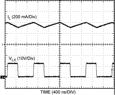
All curves taken at VIN = 12 V with configuration in typical application for driving two power LEDs with ILED = 0.35 A shown in this data sheet and TA = 25°C, unless otherwise specified.
 Figure 1. Output Current vs Input Voltage
 Figure 3. Output Current vs Input Voltage
 Figure 5. Efficiency vs Input Voltage
 Figure 7. Switch On Time vs Input Voltage
 Figure 9. VCC Voltage vs Input Voltage
 Figure 11. Switching Frequency vs RFS

| VIN = 12 V |
L = 33 µH |
fSW = 500 kHz |
Figure 13. Continuous Mode Operation

| VIN = 24 V |
L = 33 µH |
fSW = 500 kHz |
Figure 15. Continuous Mode Operation

|
VIN = 12 V |
L = 33 µH |
fSW = 1 MHz |
|
Figure 17. DIM Pin Disable Transient
 Figure 2. Output Current vs Input Voltage
 Figure 4. Efficiency vs Input Voltage
 Figure 6. Efficiency vs Input Voltage
 Figure 8. Operating Input Current vs Input Voltage
 Figure 10. Output Current vs RISNS

| VIN = 12 V |
L = 33 µH |
fSW = 1 MHz |
|
|
|
Figure 12. Continuous Mode Operation

| VIN = 24 V |
L = 33 µH |
fSW = 1 MHz |
Figure 14. Continuous Mode Operation

| VIN = 12 V |
L = 33 µH |
fSW = 1 MHz |
Figure 16. DIM Pin Enable Transient


 Figure 11. Switching Frequency vs RFS


