SNVS602L March   2009  – June 2016 LM3409 , LM3409-Q1 , LM3409HV , LM3409HV-Q1

PRODUCTION DATA.  

  1. Features
  2. Applications
  3. Description
  4. Revision History
  5. Device Comparison Table
  6. Pin Configuration and Functions
  7. Specifications
    1. 7.1 Absolute Maximum Ratings
    2. 7.2 ESD Ratings
    3. 7.3 Recommended Operating Conditions
    4. 7.4 Thermal Information
    5. 7.5 Electrical Characteristics
    6. 7.6 Typical Characteristics
  8. Detailed Description
    1. 8.1 Overview
    2. 8.2 Functional Block Diagram
    3. 8.3 Feature Description
      1. 8.3.1 Buck Current Regulators
      2. 8.3.2 Controlled Off-Time (COFT) Architecture
        1. 8.3.2.1 Adjustable Peak Current Control
        2. 8.3.2.2 Controlled Off-Time
      3. 8.3.3 Average LED Current
      4. 8.3.4 Inductor Current Ripple
      5. 8.3.5 Switching Frequency
      6. 8.3.6 PWM Dimming Using the EN Pin
      7. 8.3.7 High Voltage Negative BIAS Regulator
      8. 8.3.8 External Parallel FET PWM Dimming
    4. 8.4 Device Functional Modes
      1. 8.4.1 Low-Power Shutdown
      2. 8.4.2 Thermal Shutdown
  9. Application and Implementation
    1. 9.1 Application Information
      1. 9.1.1 Input Undervoltage Lockout (UVLO)
      2. 9.1.2 Operation Near Dropout
      3. 9.1.3 LED Ripple Current
      4. 9.1.4 Buck Converters without Output Capacitors
      5. 9.1.5 Buck Converters With Output Capacitors
      6. 9.1.6 Output Overvoltage Protection
      7. 9.1.7 Input Capacitors
      8. 9.1.8 P-Channel MOSFET (PFET)
      9. 9.1.9 Re-Circulating Diode
    2. 9.2 Typical Applications
      1. 9.2.1 EN PIN PWM Dimming Application for 10 LEDs
        1. 9.2.1.1 Design Requirements
        2. 9.2.1.2 Detailed Design Procedure
          1. 9.2.1.2.1  Nominal Switching Frequency
          2. 9.2.1.2.2  Inductor Ripple Current
          3. 9.2.1.2.3  Average LED Current
          4. 9.2.1.2.4  Output Capacitance
          5. 9.2.1.2.5  Input Capacitance
          6. 9.2.1.2.6  PFET
          7. 9.2.1.2.7  Diode
          8. 9.2.1.2.8  Input UVLO
          9. 9.2.1.2.9  IADJ Connection Method
          10. 9.2.1.2.10 PWM Dimming Method
        3. 9.2.1.3 Application Curve
      2. 9.2.2 Analog Dimming Application for 4 LEDs
        1. 9.2.2.1 Design Requirements
        2. 9.2.2.2 Detailed Design Procedure
          1. 9.2.2.2.1  Nominal Switching Frequency
          2. 9.2.2.2.2  Inductor Ripple Current
          3. 9.2.2.2.3  Average LED Current
          4. 9.2.2.2.4  Output Capacitance
          5. 9.2.2.2.5  Input Capacitance
          6. 9.2.2.2.6  PFET
          7. 9.2.2.2.7  Diode
          8. 9.2.2.2.8  Input UVLO
          9. 9.2.2.2.9  IADJ Connection Method
          10. 9.2.2.2.10 PWM Dimming Method
        3. 9.2.2.3 Application Curve
      3. 9.2.3 LM3409 Buck Converter Application
        1. 9.2.3.1 Design Requirements
        2. 9.2.3.2 Detailed Design Procedure
          1. 9.2.3.2.1  Nominal Switching Frequency
          2. 9.2.3.2.2  Inductor Ripple Current
          3. 9.2.3.2.3  Average LED Current
          4. 9.2.3.2.4  Output Capacitance
          5. 9.2.3.2.5  Input Capacitance
          6. 9.2.3.2.6  PFET
          7. 9.2.3.2.7  Diode
          8. 9.2.3.2.8  Input UVLO
          9. 9.2.3.2.9  IADJ Connection Method
          10. 9.2.3.2.10 PWM Dimming Method
  10. 10Power Supply Recommendations
  11. 11Layout
    1. 11.1 Layout Guidelines
    2. 11.2 Layout Example
  12. 12Device and Documentation Support
    1. 12.1 Device Support
      1. 12.1.1 Third-Party Products Disclaimer
    2. 12.2 Related Links
    3. 12.3 Community Resources
    4. 12.4 Trademarks
    5. 12.5 Electrostatic Discharge Caution
    6. 12.6 Glossary
  13. 13Mechanical, Packaging, and Orderable Information

Package Options

Mechanical Data (Package|Pins)
Thermal pad, mechanical data (Package|Pins)
Orderable Information

6 Pin Configuration and Functions

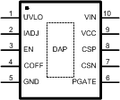
DGQ Package
10-Pin HVSSOP
Top View
LM3409 LM3409-Q1 LM3409HV LM3409HV-Q1 30085602.gif
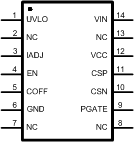
NFF Package
14-Pin PDIP
Top View
LM3409 LM3409-Q1 LM3409HV LM3409HV-Q1 300856g1.gif

Pin Functions

PIN DESCRIPTION
NAME PDIP HVSSOP
UVLO 1 1 Input undervoltage lockout. Connect to a resistor divider from VIN and GND. Turn-on threshold is 1.24 V and hysteresis for turnoff is provided by a 22 µA current source.
IADJ 3 2 Analog LED current adjust. Apply a voltage from 0 to 1.24 V, connect a resistor to GND, or leave open to set the current sense threshold voltage.
EN 4 3 Logic level enable and PWM dimming. Apply a voltage >1.74 V to enable device, a PWM signal to dim, or a voltage < 0.5 V for low-power shutdown.
COFF 5 4 Off-time programming. Connect resistor from VO, capacitor to GND to set off-time.
GND 6 5 Connect to system ground.
PGATE 9 6 Gate drive. Connect to gate of external P-channel MOSFET.
CSN 10 7 Negative current sense. Connect to negative side of sense resistor.
CSP 11 8 Positive current sense. Connect to positive side of sense resistor (also to VIN).
VCC 12 9 VIN– referenced linear regulator output. Connect at least a 1-µF ceramic capacitor to VIN. The regulator provides power for the P-channel MOSFET drive.
VIN 14 10 Input voltage. Connect to the input voltage.
Thermal pad Connect to GND pin. Place 4 to 6 vias from thermal pad to GND plane.