SNVS602L March 2009 – June 2016 LM3409 , LM3409-Q1 , LM3409HV , LM3409HV-Q1
PRODUCTION DATA.
- 1 Features
- 2 Applications
- 3 Description
- 4 Revision History
- 5 Device Comparison Table
- 6 Pin Configuration and Functions
- 7 Specifications
-
8 Detailed Description
- 8.1 Overview
- 8.2 Functional Block Diagram
- 8.3 Feature Description
- 8.4 Device Functional Modes
-
9 Application and Implementation
- 9.1
Application Information
- 9.1.1 Input Undervoltage Lockout (UVLO)
- 9.1.2 Operation Near Dropout
- 9.1.3 LED Ripple Current
- 9.1.4 Buck Converters without Output Capacitors
- 9.1.5 Buck Converters With Output Capacitors
- 9.1.6 Output Overvoltage Protection
- 9.1.7 Input Capacitors
- 9.1.8 P-Channel MOSFET (PFET)
- 9.1.9 Re-Circulating Diode
- 9.2
Typical Applications
- 9.2.1 EN PIN PWM Dimming Application for 10 LEDs
- 9.2.2 Analog Dimming Application for 4 LEDs
- 9.2.3 LM3409 Buck Converter Application
- 9.1
Application Information
- 10Power Supply Recommendations
- 11Layout
- 12Device and Documentation Support
- 13Mechanical, Packaging, and Orderable Information
Package Options
Mechanical Data (Package|Pins)
Thermal pad, mechanical data (Package|Pins)
- DGQ|10
Orderable Information
11 Layout
11.1 Layout Guidelines
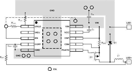
The performance of any switching converter depends as much upon the layout of the PCB as the component selection. Following a few simple guidelines will maximimize noise rejection and minimize the generation of EMI within the circuit.
Discontinuous currents are the most likely to generate EMI, therefore take care when routing these paths. The main path for discontinuous current in the LM3409/09HV buck converter contains the input capacitor (CIN), the recirculating diode (D1), the P-channel MOSFET (Q1), and the sense resistor (RSNS). This loop should be kept as small as possible and the connections between all three components should be short and thick to minimize parasitic inductance. In particular, the switch node (where L1, D1 and Q1 connect) should be just large enough to connect the components without excessive heating from the current it carries.
The IADJ, COFF, CSN and CSP pins are all high-impedance control inputs which couple external noise easily, therefore the loops containing these high impedance nodes should be minimized. The most sensitive loop contains the sense resistor (RSNS) which should be placed as close as possible to the CSN and CSP pins to maximize noise rejection. The off-time capacitor (COFF) should be placed close to the COFF and GND pins for the same reason. Finally, if an external resistor (REXT) is used to bias the IADJ pin, it should be placed close to the IADJ and GND pins, also.
In some applications the LED or LED array can be far away (several inches or more) from the LM3409/09HV, or on a separate PCB connected by a wiring harness. When an output capacitor is used and the LED array is large or separated from the rest of the converter, the output capacitor should be placed close to the LEDs to reduce the effects of parasitic inductance on the AC impedance of the capacitor.
11.2 Layout Example
 Figure 34. Layout Recommendation