SNVS678F June   2010  – November 2015 LM3414 , LM3414HV

PRODUCTION DATA.  

  1. Features
  2. Applications
  3. Description
  4. Revision History
  5. Pin Configuration and Functions
  6. Specifications
    1. 6.1 Absolute Maximum Ratings
    2. 6.2 ESD Ratings
    3. 6.3 Recommended Operating Conditions
    4. 6.4 Thermal Information
    5. 6.5 Electrical Characteristics
    6. 6.6 Typical Characteristics
  7. Detailed Description
    1. 7.1 Overview
    2. 7.2 Functional Block Diagram
    3. 7.3 Feature Description
      1. 7.3.1 Pulse-Level-Modulation (PLM) Operation Principles
      2. 7.3.2 Minimum Switch ON-time
      3. 7.3.3 Peak Switch Current Limit
      4. 7.3.4 PWM Dimming Control
      5. 7.3.5 Analog Dimming Control
      6. 7.3.6 Internal VCC Regulator
    4. 7.4 Device Functional Modes
  8. Application and Implementation
    1. 8.1 Application Information
      1. 8.1.1 Setting the Switching Frequency
      2. 8.1.2 Setting LED Current
      3. 8.1.3 Inductor Selection
    2. 8.2 Typical Applications
      1. 8.2.1 LM3414/HV Design Example
        1. 8.2.1.1 Design Requirements
        2. 8.2.1.2 Detailed Design Procedure
          1. 8.2.1.2.1 Calculate Operating Parameters
          2. 8.2.1.2.2 Calculate RIADJ
          3. 8.2.1.2.3 Calculate RFS
          4. 8.2.1.2.4 Calculate LMIN
          5. 8.2.1.2.5 Calculate CIN-MIN
      2. 8.2.2 LM3414/HV Design Example (IOUT = 1 A)
        1. 8.2.2.1 Design Requirements
        2. 8.2.2.2 Detailed Design Procedure
          1. 8.2.2.2.1 Calculate Operating Parameters
          2. 8.2.2.2.2 Calculate RIADJ
          3. 8.2.2.2.3 Calculate RFS
          4. 8.2.2.2.4 Calculate LMIN
          5. 8.2.2.2.5 Calculate CIN-MIN
        3. 8.2.2.3 Application Curve
  9. Power Supply Recommendations
  10. 10Layout
    1. 10.1 Layout Guidelines
    2. 10.2 Layout Example
  11. 11Device and Documentation Support
    1. 11.1 Related Links
    2. 11.2 Community Resources
    3. 11.3 Trademarks
    4. 11.4 Electrostatic Discharge Caution
    5. 11.5 Glossary
  12. 12Mechanical, Packaging, and Orderable Information

Package Options

Mechanical Data (Package|Pins)
Thermal pad, mechanical data (Package|Pins)
Orderable Information

10 Layout

10.1 Layout Guidelines

Discontinuous currents are the most likely to generate EMI; therefore, take care when routing these paths. The main path for discontinuous current in the LM3414/HV buck converter contains the input capacitor (CIN), the recirculating diode (D1), and the switch node (LX). This loop should be kept as small as possible and the connections between all three components should be short and thick to minimize parasitic inductance. In particular, the switch node (where L1, D1 and LX connect) should be just large enough to connect the components without excessive heating from the current it carries.

The IADJ, FS, and DIM pins are all high-impedance control inputs which couple external noise easily, therefore the loops containing these high impedance nodes should be minimized. The frequency setting resistor (RFS) and current setting resistor (RIADJ) should be placed close to the FS and IADJ pins as possible.

10.2 Layout Example
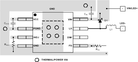
LM3414 LM3414HV snvs678_layout.gif Figure 25. Layout Recommendation