SNVS678F June 2010 – November 2015 LM3414 , LM3414HV
PRODUCTION DATA.
- 1 Features
- 2 Applications
- 3 Description
- 4 Revision History
- 5 Pin Configuration and Functions
- 6 Specifications
- 7 Detailed Description
- 8 Application and Implementation
- 9 Power Supply Recommendations
- 10Layout
- 11Device and Documentation Support
- 12Mechanical, Packaging, and Orderable Information
Package Options
Mechanical Data (Package|Pins)
Thermal pad, mechanical data (Package|Pins)
- DDA|8
Orderable Information
5 Pin Configuration and Functions
DDA Package
8-Pin SOIC
Top View

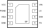
NGQ Package
8-Pin WSON
Top View

Pin Functions
| PIN | I/O | DESCRIPTION | |
|---|---|---|---|
| NAME | NO. | ||
| VCC | 1 | O | Internal Regulator Output Pin. This pin should be bypassed to ground by a ceramic capacitor with a minimum value of 1 µF. |
| PGND | 2 | — | Power Ground Pin. Ground for power circuitry. Reference point for all stated voltages. Must be externally connected to EP and GND. |
| IADJ | 3 | I | Average Output Current Adjustment Pin. Connect resistor RIADJ from this pin to ground to adjust the average output current. |
| GND | 4 | — | Analog Ground Pin. Analog ground connection for internal circuitry, must be connected to PGND external to the package. |
| FS | 5 | I | Switching Frequency Setting Pin. Connect resistor RFS from this pin to ground to set the switching frequency. |
| DIM | 6 | I | PWM Dimming Control Pin. Apply logic level PWM signal to this pin controls the intend brightness of the LED string. |
| LX | 7 | O | Drain of N-MOSFET Switch. Connect this pin to the output inductor and anode of the schottky diode. |
| VIN | 8 | I | Input Voltage Pin. The input voltage should be in the range of 4.5 V to 42 V (LM3414) or 4.5 V to 65 V (LM3414HV). |
| EP | EP | — | Thermal Pad (Power Ground). Used to dissipate heat from the package during operation. Must be electrically connected to PGND external to the package. |