SNVS678F June 2010 – November 2015 LM3414 , LM3414HV
PRODUCTION DATA.
- 1 Features
- 2 Applications
- 3 Description
- 4 Revision History
- 5 Pin Configuration and Functions
- 6 Specifications
- 7 Detailed Description
- 8 Application and Implementation
- 9 Power Supply Recommendations
- 10Layout
- 11Device and Documentation Support
- 12Mechanical, Packaging, and Orderable Information
Package Options
Mechanical Data (Package|Pins)
Thermal pad, mechanical data (Package|Pins)
- DDA|8
Orderable Information
6 Specifications
6.1 Absolute Maximum Ratings
over operating free-air temperature range (unless otherwise noted)(1)| MIN | MAX | UNIT | ||
|---|---|---|---|---|
| VIN to GND | LM3414 | –0.3 | 42 | V |
| LM3414HV | –0.3 | 65 | ||
| VIN to GND (Transient) | LM3414 | 45 (500 ms) | V | |
| LM3414HV | 67 (500 ms) | |||
| LX to PGND | LM3414 | –0.3 | 42 | V |
| LM3414HV | –0.3 | 65 | ||
| LX to PGND (Transient) | LM3414 | –3 (2 ns) | 45 (500 ms) | V |
| LM3414HV | –3 (2 ns) | 67 (500 ms) | ||
| FS, IADJ to GND | –0.3 | 5 | V | |
| DIM to GND | –0.3 | 6 | V | |
| Storage Temperature | –65 | 125 | °C | |
(1) Stresses beyond those listed under Absolute Maximum Ratings may cause permanent damage to the device. These are stress ratings only, which do not imply functional operation of the device at these or any other conditions beyond those indicated under Recommended Operating Conditions. Exposure to absolute-maximum-rated conditions for extended periods may affect device reliability.
6.2 ESD Ratings
| VALUE | UNIT | |||
|---|---|---|---|---|
| WSON PACKAGE | ||||
| V(ESD) | Electrostatic discharge | Human-body model (HBM), per ANSI/ESDA/JEDEC JS-001(1)(3) | ±2000 | V |
| Charged-device model (CDM), per JEDEC specification JESD22-C101(2) | ±750 | |||
| SOIC PACKAGE | ||||
| V(ESD) | Electrostatic discharge | Human-body model (HBM), per ANSI/ESDA/JEDEC JS-001(1)(3) | ±2000 | V |
| Charged-device model (CDM), per JEDEC specification JESD22-C101(2) | ±750 | |||
(1) JEDEC document JEP155 states that 500-V HBM allows safe manufacturing with a standard ESD control process.
(2) JEDEC document JEP157 states that 250-V CDM allows safe manufacturing with a standard ESD control process.
(3) The human body model is a 100pF capacitor discharged through a 1.5 kΩ resistor into each pin.
6.3 Recommended Operating Conditions
over operating free-air temperature range (unless otherwise noted)| MIN | NOM | MAX | UNIT | ||
|---|---|---|---|---|---|
| VIN | LM3414 | 4.5 | 42 | V | |
| LM3414HV | 4.5 | 65 | |||
| Junction temperature | –40 | 125 | °C | ||
6.4 Thermal Information
| THERMAL METRIC(1) | LM3414, LM3414HV | UNIT | ||
|---|---|---|---|---|
| NGQ (WSON) | DDA (SOIC-8) | |||
| 8 PINS | 8 PINS | |||
| RθJA | Junction-to-ambient thermal resistance | 47.7 | 50.5 | °C/W |
| RθJC(top) | Junction-to-case (top) thermal resistance | 43.1 | 55.7 | °C/W |
| RθJB | Junction-to-board thermal resistance | 22.3 | 28.6 | °C/W |
| ψJT | Junction-to-top characterization parameter | 0.4 | 9.5 | °C/W |
| ψJB | Junction-to-board characterization parameter | 22.5 | 28.5 | °C/W |
| RθJC(bot) | Junction-to-case (bottom) thermal resistance | 4 | 3.2 | °C/W |
(1) For more information about traditional and new thermal metrics, see the Semiconductor and IC Package Thermal Metrics application report, SPRA953.
6.5 Electrical Characteristics
MIN and MAX limits apply for TJ = –40°C to 125°C unless specified otherwise. VIN = 24 V unless otherwise indicated.| PARAMETER | TEST CONDITIONS | MIN(1) | TYP(2) | MAX(1) | UNIT | |
|---|---|---|---|---|---|---|
| SYSTEM PARAMETERS - LM3414 | ||||||
| IIN-DIM-HIGH | Operating Current | 4.5 V ≤ Vin ≤ 42 V RIADJ = 3.125 kΩ VDIM = High |
2.2 | 3.2 | 3.5 | mA |
| IIN-DIM-LOW | Standby Current | 4.5 V ≤ Vin ≤ 42 V RIADJ = 3.125 kΩ VDIM = Low |
0.8 | 1.15 | 1.4 | mA |
| ILX-OFF | LX Pin Current | Main Switch Turned OFF VLX = VIN = 42 V |
6 | µA | ||
| SYSTEM PARAMETERS - LM3414HV | ||||||
| IIN-DIM-HIGH | Operating Current | 4.5 V ≤ Vin ≤ 65 V RIADJ = 3.125 kΩ VDIM = High |
2.2 | 3.3 | 3.6 | mA |
| IIN-DIM-LOW | Standby Current | 4.5 V ≤ Vin ≤ 65 V RIADJ = 3.125 kΩ VDIM = Low |
0.8 | 1.2 | 1.45 | mA |
| ILX-OFF | LX Pin Current | Main Switch Turned OFF VLX = VIN= 65 V |
6.5 | µA | ||
| SYSTEM PARAMETERS - LM3414/3414HV | ||||||
| ILED | Average LED Current | RIADJ = 3.125 kΩ TA = 25°C |
0.97 | 1 | 1.03 | A |
| RIADJ = 3.125 kΩ TA = –40°C to 125°C |
0.95 | 1 | 1.05 | A | ||
| VCC-UVLO | Vcc UVLO Threshold | VCC Decreasing, TA = 25°C | 3.6 | 3.75 | 3.9 | V |
| VCC-UVLO-HYS | Vcc UVLO Hysteresis | 300 | mV | |||
| VIADJ | IADJ Pin voltage | 1.23 | 1.255 | 1.280 | V | |
| VDIM | DIM Pin Threshold | VDIM Increasing | 1 | 1.2 | V | |
| VDIM-HYS | DIM Pin Hysteresis | 100 | mV | |||
| fSW | Switching frequency | 250 | 500 | 1000 | kHz | |
| fSW-TOL | Switching frequency tolerance | RFS = 40 kΩ | 420 | 500 | 580 | kHz |
| tON-MIN | Minimum on-time | 400 | ns | |||
| INTERNAL VOLTAGE REGULATOR | ||||||
| VCC | VCC regulator output voltage(3) | CVCC = 1 µF, No Load to IVCC = 2 mA | 4.7 | 5.4 | 6 | V |
| VIN = 4.5 V, 2-mA Load | 3.8 | 4.2 | V | |||
| MAIN SWITCH | ||||||
| RLX | Resistance across LX and GND | Main Switch Turned ON | 1.8 | Ω | ||
| THERMAL PROTECTION | ||||||
| TSD | Thermal shutdown temperature | TJ Rising | 170 | °C | ||
| TSD-HYS | Thermal shutdown temperature hysteresis | TJ Falling | 10 | °C | ||
(1) All limits specified at room temperature (TYP) and at temperature extremes (MIN/MAX). All room temperature limits are 100% production tested. All limits at temperature extremes are specified through correlation using standard Statistical Quality Control (SQC) methods. All limits are used to calculate Average Outgoing Quality Level (AOQL).
(2) Typical specification represent the most likely parametric norm at 25°C operation.
(3) VCC provides self bias for the internal gate drive and control circuits. Device thermal limitations limit external loading to the pin.
6.6 Typical Characteristics
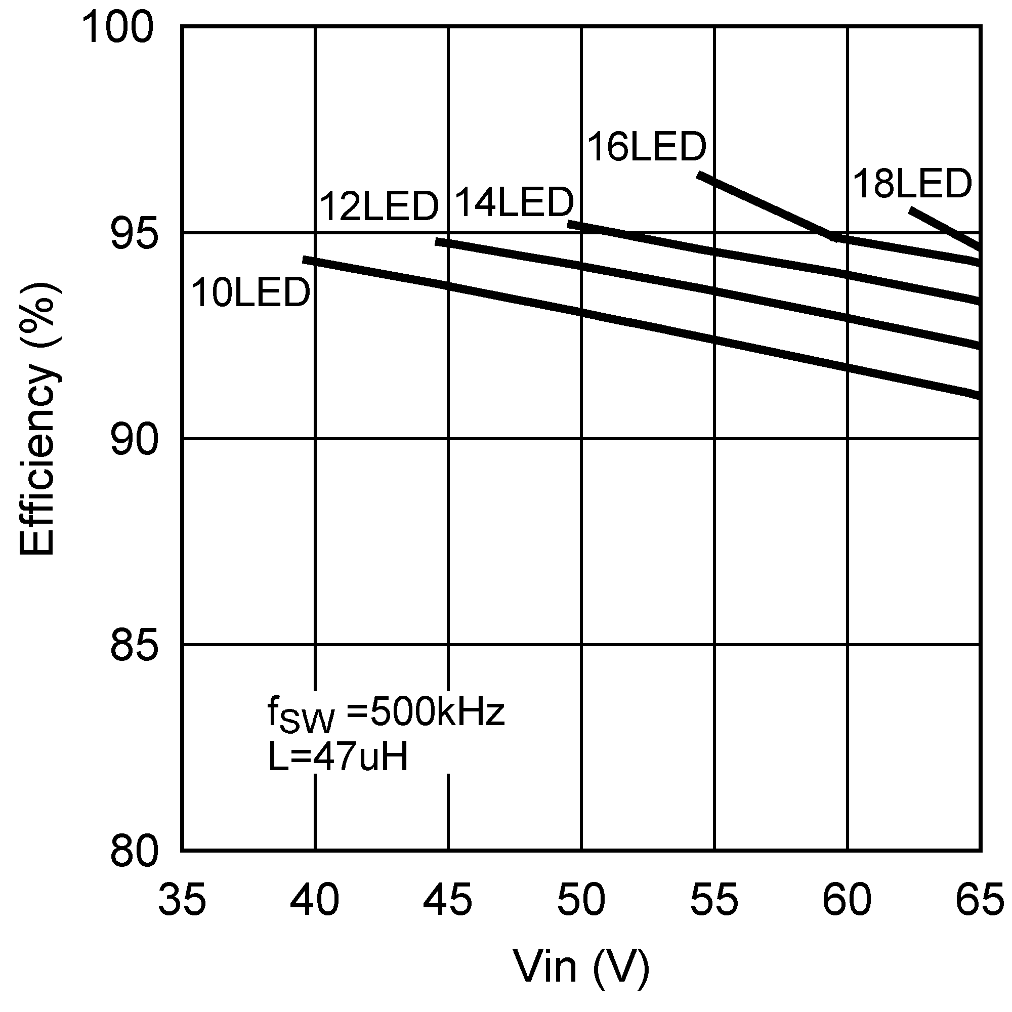
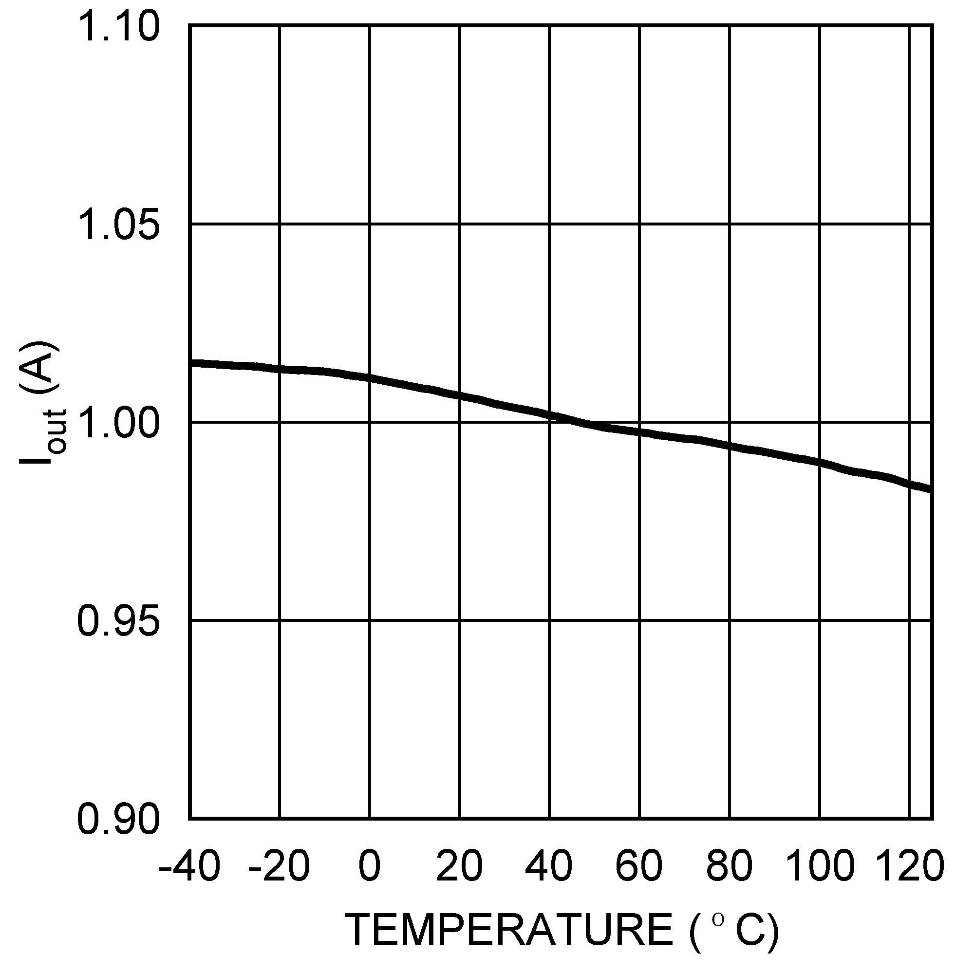
All curves taken at VIN = 48 V with configuration in typical application for driving twelve power LEDs with ILED = 1 A shown in this data sheet. TA = 25°C, unless otherwise specified.


(6 LED, VIN = 24 V), LM3414HV


(12 LED, VIN = 48 V), LM3414HV


