SNVSB95 July 2019 LM3421-Q1 , LM3423-Q1
PRODUCTION DATA.
- 1 Features
- 2 Applications
- 3 Description
- 4 Revision History
- 5 Device Comparison
- 6 Pin Configuration and Functions
- 7 Specifications
-
8 Detailed Description
- 8.1 Overview
- 8.2 Functional Block Diagram
- 8.3
Feature Description
- 8.3.1 Current Regulators
- 8.3.2 Predictive Off-Time (PRO) Control
- 8.3.3 Average LED Current
- 8.3.4 Analog Dimming
- 8.3.5 Current Sense and Current Limit
- 8.3.6 Overcurrent Protection
- 8.3.7 Zero Current Shutdown
- 8.3.8 Control Loop Compensation
- 8.3.9 Start-Up Regulator
- 8.3.10 Overvoltage Lockout (OVLO)
- 8.3.11 Input Undervoltage Lockout (UVLO)
- 8.3.12 PWM Dimming
- 8.3.13 LM3423-Q1 Only: DPOL, FLT, TIMR, and LRDY
-
9 Application and Implementation
- 9.1 Application Information
- 9.2
Typical Applications
- 9.2.1
Basic Topology Schematics
- 9.2.1.1 Design Requirements
- 9.2.1.2
Detailed Design Procedure
- 9.2.1.2.1 Operating Point
- 9.2.1.2.2 Switching Frequency
- 9.2.1.2.3 Average LED Current
- 9.2.1.2.4 Inductor Ripple Current
- 9.2.1.2.5 LED Ripple Current
- 9.2.1.2.6 Peak Current Limit
- 9.2.1.2.7 Loop Compensation
- 9.2.1.2.8 Input Capacitance
- 9.2.1.2.9 N-channel FET
- 9.2.1.2.10 Diode
- 9.2.1.2.11 Output OVLO
- 9.2.1.2.12 Input UVLO
- 9.2.1.2.13 PWM Dimming Method
- 9.2.1.2.14 Analog Dimming Method
- 9.2.2
LM3421 Buck-Boost Application
- 9.2.2.1 Design Requirements
- 9.2.2.2
Detailed Design Procedure
- 9.2.2.2.1 Operating Point
- 9.2.2.2.2 Switching Frequency
- 9.2.2.2.3 Average LED Current
- 9.2.2.2.4 Inductor Ripple Current
- 9.2.2.2.5 Output Capacitance
- 9.2.2.2.6 Peak Current Limit
- 9.2.2.2.7 Loop Compensation
- 9.2.2.2.8 Input Capacitance
- 9.2.2.2.9 N-channel FET
- 9.2.2.2.10 Diode
- 9.2.2.2.11 Input UVLO
- 9.2.2.2.12 Output OVLO
- 9.2.2.3 Application Curve
- 9.2.3 LM3421-Q1 BOOST Application
- 9.2.4 LM3421-Q1 Buck-Boost Application
- 9.2.5 LM3423-Q1 Boost Application
- 9.2.6 LM3421 Buck-Boost Application
- 9.2.7 LM3423 Buck Application
- 9.2.8 LM3423 Buck-Boost Application
- 9.2.9 LM3421 SEPIC Application
- 9.2.1
Basic Topology Schematics
- 10Power Supply Recommendations
- 11Layout
- 12Device and Documentation Support
- 13Mechanical, Packaging, and Orderable Information
Package Options
Mechanical Data (Package|Pins)
- PWP|16
Thermal pad, mechanical data (Package|Pins)
- PWP|16
Orderable Information
9.1.7 Boost Inrush Current
When configured as a boost converter, there is a phantom power path comprised of the inductor, the output diode, and the output capacitor. This path causes two things to happen when power is applied:
- a very large inrush of current to charge the output capacitor
- the energy stored in the inductor during this inrush collects in the output capacitor, charging it to a higher potential than the input voltage
Depending on the state of the EN pin, the output capacitor discharges by:
- EN < 1.3 V: no discharge path (leakage only).
- EN > 1.3 V, the OVP divider resistor path, if present, and 10 µA into each of the HSP & HSN pins.
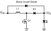
In applications using the OVP divider and with EN > 1.3 V, the output capacitor voltage can charge higher than VTURN-OFF. In this situation, the FLT pin (LM3423-Q1 only) is open and the PWM dimming MOSFET is turned off. This condition (the system appearing disabled) can persist for an undesirably long time. Possible solutions to this condition include:
- Add an inrush diode from VIN to the output as shown in Figure 30.
- Add an NTC thermistor in series with the input to prevent the inrush from overcharging the output capacitor too high.
- Use a current limited source supply.
- Raise the OVP threshold.
 Figure 30. Boost Topology with Inrush Diode