SNVSB95 July 2019 LM3421-Q1 , LM3423-Q1
PRODUCTION DATA.
- 1 Features
- 2 Applications
- 3 Description
- 4 Revision History
- 5 Device Comparison
- 6 Pin Configuration and Functions
- 7 Specifications
-
8 Detailed Description
- 8.1 Overview
- 8.2 Functional Block Diagram
- 8.3
Feature Description
- 8.3.1 Current Regulators
- 8.3.2 Predictive Off-Time (PRO) Control
- 8.3.3 Average LED Current
- 8.3.4 Analog Dimming
- 8.3.5 Current Sense and Current Limit
- 8.3.6 Overcurrent Protection
- 8.3.7 Zero Current Shutdown
- 8.3.8 Control Loop Compensation
- 8.3.9 Start-Up Regulator
- 8.3.10 Overvoltage Lockout (OVLO)
- 8.3.11 Input Undervoltage Lockout (UVLO)
- 8.3.12 PWM Dimming
- 8.3.13 LM3423-Q1 Only: DPOL, FLT, TIMR, and LRDY
-
9 Application and Implementation
- 9.1 Application Information
- 9.2
Typical Applications
- 9.2.1
Basic Topology Schematics
- 9.2.1.1 Design Requirements
- 9.2.1.2
Detailed Design Procedure
- 9.2.1.2.1 Operating Point
- 9.2.1.2.2 Switching Frequency
- 9.2.1.2.3 Average LED Current
- 9.2.1.2.4 Inductor Ripple Current
- 9.2.1.2.5 LED Ripple Current
- 9.2.1.2.6 Peak Current Limit
- 9.2.1.2.7 Loop Compensation
- 9.2.1.2.8 Input Capacitance
- 9.2.1.2.9 N-channel FET
- 9.2.1.2.10 Diode
- 9.2.1.2.11 Output OVLO
- 9.2.1.2.12 Input UVLO
- 9.2.1.2.13 PWM Dimming Method
- 9.2.1.2.14 Analog Dimming Method
- 9.2.2
LM3421 Buck-Boost Application
- 9.2.2.1 Design Requirements
- 9.2.2.2
Detailed Design Procedure
- 9.2.2.2.1 Operating Point
- 9.2.2.2.2 Switching Frequency
- 9.2.2.2.3 Average LED Current
- 9.2.2.2.4 Inductor Ripple Current
- 9.2.2.2.5 Output Capacitance
- 9.2.2.2.6 Peak Current Limit
- 9.2.2.2.7 Loop Compensation
- 9.2.2.2.8 Input Capacitance
- 9.2.2.2.9 N-channel FET
- 9.2.2.2.10 Diode
- 9.2.2.2.11 Input UVLO
- 9.2.2.2.12 Output OVLO
- 9.2.2.3 Application Curve
- 9.2.3 LM3421-Q1 BOOST Application
- 9.2.4 LM3421-Q1 Buck-Boost Application
- 9.2.5 LM3423-Q1 Boost Application
- 9.2.6 LM3421 Buck-Boost Application
- 9.2.7 LM3423 Buck Application
- 9.2.8 LM3423 Buck-Boost Application
- 9.2.9 LM3421 SEPIC Application
- 9.2.1
Basic Topology Schematics
- 10Power Supply Recommendations
- 11Layout
- 12Device and Documentation Support
- 13Mechanical, Packaging, and Orderable Information
Package Options
Mechanical Data (Package|Pins)
- PWP|16
Thermal pad, mechanical data (Package|Pins)
- PWP|16
Orderable Information
8.3.1 Current Regulators
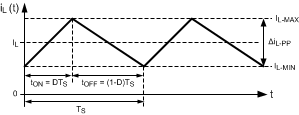
 Figure 12. Ideal CCM Regulator Inductor Current iL(t)
 Current regulators can create three basic topologies: buck, boost, or buck-boost. All three topologies in their most basic form contain a main switching MOSFET, a recirculating diode, an inductor and capacitors. The controller is designed to drive a ground referenced N-channel FET which is perfect for a standard boost regulator. However, buck and buck-boost regulators usually have a high-side switch. When driving an LED load, a ground referenced load is often not necessary, therefore a ground referenced switch drives a floating load instead. The controller can then be used to drive all three basic topologies as shown in the Basic Topology Schematics section. Other topologies such as the SEPIC and flyback converter (both derivatives of the buck-boost) can be implemented as well.
Looking at the buck-boost design, the basic operation of a current regulator can be analyzed. During the time that the N-channel FET (Q1) is turned on (tON), the input voltage source stores energy in the inductor (L1) while the output capacitor (CO) provides energy to the LED load. When Q1 is turned off (tOFF), the re-circulating diode (D1) becomes forward biased and L1 provides energy to both CO and the LED load. Figure 12 shows the inductor current (iL(t)) waveform for a regulator operating in CCM.
The average output LED current (ILED) is proportional to the average inductor current (IL) , therefore if IL is tightly controlled, ILED is well regulated. As the system changes input voltage or output voltage, the ideal duty cycle (D) is varied to regulate IL and ultimately ILED. For any current regulator, D is a function of the conversion ratio:
Buck

Boost

Buck-boost
