SNVSB96 July 2019 LM3424-Q1
PRODUCTION DATA.
- 1 Features
- 2 Applications
- 3 Description
- 4 Revision History
- 5 Pin Configuration and Functions
- 6 Specifications
-
7 Detailed Description
- 7.1 Overview
- 7.2 Functional Block Diagram
- 7.3
Feature Description
- 7.3.1 Current Regulators
- 7.3.2 Peak Current Mode Control
- 7.3.3 Average LED Current
- 7.3.4 Thermal Foldback and Analog Dimming
- 7.3.5 Current Sense and Current Limit
- 7.3.6 Slope Compensation
- 7.3.7 Control Loop Compensation
- 7.3.8 Start-Up Regulator and Soft-Start
- 7.3.9 Overvoltage Lockout (OVLO)
- 7.3.10 Input Undervoltage Lockout (UVLO)
- 7.3.11 PWM Dimming
- 7.3.12 Thermal Shutdown
- 7.4 Device Functional Modes
-
8 Application and Implementation
- 8.1 Application Information
- 8.2
Typical Applications
- 8.2.1
Basic Topology Schematics
- 8.2.1.1 Design Requirements
- 8.2.1.2
Detailed Design Procedure
- 8.2.1.2.1 Operating Point
- 8.2.1.2.2 Switching Frequency
- 8.2.1.2.3 Average LED Current
- 8.2.1.2.4 Thermal Foldback
- 8.2.1.2.5 Inductor Ripple Current
- 8.2.1.2.6 LED Ripple Current
- 8.2.1.2.7 Peak Current Limit
- 8.2.1.2.8 Slope Compensation
- 8.2.1.2.9 Loop Compensation
- 8.2.1.2.10 Input Capacitance
- 8.2.1.2.11 NFET
- 8.2.1.2.12 Diode
- 8.2.1.2.13 Output OVLO
- 8.2.1.2.14 Input UVLO
- 8.2.1.2.15 Soft-Start
- 8.2.1.2.16 PWM Dimming Method
- 8.2.1.2.17 Analog Dimming Method
- 8.2.2
Buck-Boost Application
- 8.2.2.1 Design Requirements
- 8.2.2.2
Detailed Design Procedure
- 8.2.2.2.1 Operating Point
- 8.2.2.2.2 Switching Frequency
- 8.2.2.2.3 Average LED Current
- 8.2.2.2.4 Thermal Foldback
- 8.2.2.2.5 Inductor Ripple Current
- 8.2.2.2.6 Output Capacitance
- 8.2.2.2.7 Peak Current Limit
- 8.2.2.2.8 Slope Compensation
- 8.2.2.2.9 Loop Compensation
- 8.2.2.2.10 Input Capacitance
- 8.2.2.2.11 NFET
- 8.2.2.2.12 Diode
- 8.2.2.2.13 Input UVLO
- 8.2.2.2.14 Output OVLO
- 8.2.2.2.15 Soft-Start
- 8.2.2.3 Application Curve
- 8.2.3 Boost Application
- 8.2.4 Buck-Boost Application
- 8.2.5 Boost Application
- 8.2.6 Buck-Boost Application
- 8.2.7 Buck Application
- 8.2.8 Buck-Boost Application
- 8.2.9 SEPIC Application
- 8.2.1
Basic Topology Schematics
- 9 Power Supply Recommendations
- 10Layout
- 11Device and Documentation Support
- 12Mechanical, Packaging, and Orderable Information
Package Options
Mechanical Data (Package|Pins)
- PWP|20
Thermal pad, mechanical data (Package|Pins)
- PWP|20
Orderable Information
8.2.1.2.9 Loop Compensation
Using a simple first order peak current mode control model, neglecting any output capacitor ESR dynamics, the necessary loop compensation can be determined.
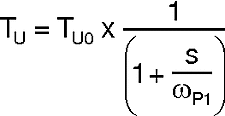
First, the uncompensated loop gain (TU) of the regulator can be approximated:
Buck

Boost and Buck-Boost

Where the pole (ωP1) is approximated:
Buck

Boost

Buck-Boost

And the RHP zero (ωZ1) is approximated:
Boost

Buck-Boost

And the uncompensated DC loop gain (TU0) is approximated:
Buck

Boost

Buck-Boost

For all topologies, the primary method of compensation is to place a low frequency dominant pole (ωP2) which will ensure that there is ample phase margin at the crossover frequency. This is accomplished by placing a capacitor (CCMP) from the COMP pin to GND, which is calculated according to the lower value of the pole and the RHP zero of the system (shown as a minimizing function):


If analog dimming is used, CCMP should be approximately 4x larger to maintain stability as the LEDs are dimmed to zero.
A high frequency compensation pole (ωP3) can be used to attenuate switching noise and provide better gain margin. Assuming RFS = 10Ω, CFS is calculated according to the higher value of the pole and the RHP zero of the system (shown as a maximizing function):


The total system loop gain (T) can then be written as:
Buck

Boost and Buck-Boost
