SNVS616H April 2009 – July 2015 LM3429 , LM3429-Q1
PRODUCTION DATA.
- 1 Features
- 2 Applications
- 3 Description
- 4 Revision History
- 5 Pin Configuration and Functions
- 6 Specifications
-
7 Detailed Description
- 7.1 Overview
- 7.2 Functional Block Diagram
- 7.3
Feature Description
- 7.3.1 Current Regulators
- 7.3.2 Predictive Off-Time (PRO) Control
- 7.3.3 Switching Frequency
- 7.3.4 Average LED Current
- 7.3.5 Analog Dimming
- 7.3.6 Current Sense and Current Limit
- 7.3.7 Control Loop Compensation
- 7.3.8 Output Overvoltage Lockout (OVLO)
- 7.3.9 Input Undervoltage Lockout (UVLO)
- 7.3.10 PWM Dimming
- 7.3.11 Startup Regulator (VCC LDO)
- 7.3.12 Thermal Shutdown
- 7.4 Device Functional Modes
-
8 Application and Implementation
- 8.1 Application Information
- 8.2
Typical Applications
- 8.2.1
Basic Topology Schematics
- 8.2.1.1 Design Requirements
- 8.2.1.2
Detailed Design Procedure
- 8.2.1.2.1 Operating Point
- 8.2.1.2.2 Switching Frequency
- 8.2.1.2.3 Average LED Current
- 8.2.1.2.4 Inductor Ripple Current
- 8.2.1.2.5 LED Ripple Current
- 8.2.1.2.6 Peak Current Limit
- 8.2.1.2.7 Loop Compensation
- 8.2.1.2.8 Input Capacitance
- 8.2.1.2.9 NFET
- 8.2.1.2.10 Diode
- 8.2.1.2.11 Output OVLO
- 8.2.1.2.12 Input UVLO
- 8.2.1.2.13 PWM Dimming Method
- 8.2.1.2.14 Analog Dimming Method
- 8.2.2
Buck-Boost Application - 6 LEDs at 1 A
- 8.2.2.1 Design Requirements
- 8.2.2.2
Detailed Design Procedure
- 8.2.2.2.1 Operating Point
- 8.2.2.2.2 Switching Frequency
- 8.2.2.2.3 Average LED Current
- 8.2.2.2.4 Inductor Ripple Current
- 8.2.2.2.5 Output Capacitance
- 8.2.2.2.6 Peak Current Limit
- 8.2.2.2.7 Loop Compensation
- 8.2.2.2.8 Input Capacitance
- 8.2.2.2.9 NFET
- 8.2.2.2.10 Diode
- 8.2.2.2.11 Input UVLO
- 8.2.2.2.12 Output OVLO
- 8.2.2.3 Application Curve
- 8.2.3 Boost PWM Dimming Application - 9 LEDs at 1 A
- 8.2.4 Buck-Boost Analog Dimming Application - 4 LEDs at 2A
- 8.2.5 Boost Analog Dimming Application - 12 LEDs at 700 mA
- 8.2.6 Buck-Boost PWM Dimming Application - 6 LEDs at 500 mA
- 8.2.7 Buck Application - 3 LEDS at 1.25 A
- 8.2.8 Buck-Boost Thermal Foldback Application - 8 LEDs at 2.5 A
- 8.2.9 SEPIC Application - 5 LEDs at 750 mA
- 8.2.1
Basic Topology Schematics
- 9 Power Supply Recommendations
- 10Layout
- 11Device and Documentation Support
- 12Mechanical, Packaging, and Orderable Information
Package Options
Mechanical Data (Package|Pins)
- PWP|14
Thermal pad, mechanical data (Package|Pins)
- PWP|14
Orderable Information
7 Detailed Description
7.1 Overview
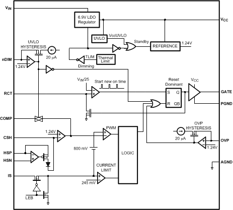
The LM3429 is an N-channel MosFET (NFET) controller for buck, boost and buck-boost current regulators which are ideal for driving LED loads. The controller has wide input voltage range allowing for regulation of a variety of LED loads. The high-side differential current sense, with low adjustable threshold voltage, provides an excellent method for regulating output current while maintaining high system efficiency. The LM3429 uses a Predictive Off-time (PRO) control architecture that allows the regulator to be operated using minimal external control loop compensation, while providing an inherent cycle-by-cycle current limit. The adjustable current sense threshold provides the capability to amplitude (analog) dim the LED current and the output enable/disable function allows for PWM dimming using no external components. When designing, the maximum attainable LED current is not internally limited because the LM3429 is a controller. Instead it is a function of the system operating point, component choices, and switching frequency allowing the LM3429 to easily provide constant currents up to 5A. This simple controller contains all the features necessary to implement a high-efficiency versatile LED driver.
7.2 Functional Block Diagram
7.3 Feature Description
7.3.1 Current Regulators
Current regulators can be designed to accomplish three basic functions: buck, boost, and buck-boost. All three topologies in their most basic form contain a main switching MosFET, a recirculating diode, an inductor and capacitors. The LM3429 is designed to drive a ground referenced NFET which is perfect for a standard boost regulator. Buck and buck-boost regulators, on the other hand, usually have a high-side switch. When driving an LED load, a ground referenced load is often not necessary, therefore a ground referenced switch can be used to drive a floating load instead. The LM3429 can then be used to drive all three basic topologies as shown in the Typical Applications section.
Looking at the buck-boost design, the basic operation of a current regulator can be analyzed. During the time that the NFET (Q1) is turned on (tON), the input voltage source stores energy in the inductor (L1) while the output capacitor (CO) provides energy to the LED load. When Q1 is turned off (tOFF), the re-circulating diode (D1) becomes forward biased and L1 provides energy to both CO and the LED load. Figure 12 shows the inductor current (iL(t)) waveform for a regulator operating in CCM.
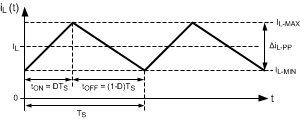 Figure 12. Ideal CCM Regulator Inductor Current iL(t)
The average output LED current (ILED) is proportional to the average inductor current (IL) , therefore if IL is tightly controlled, ILED will be well regulated. As the system changes input voltage or output voltage, the ideal duty cycle (D) is varied to regulate IL and ultimately ILED. For any current regulator, D is a function of the conversion ratio:
Buck

Boost

Buck-Boost

7.3.2 Predictive Off-Time (PRO) Control
PRO control is used by the LM3429 to control ILED. It is a combination of average peak current control and a one-shot off-timer that varies with input voltage. The LM3429 uses peak current control to regulate the average LED current through an array of HBLEDs. This method of control uses a series resistor in the LED path to sense LED current and can use either a series resistor in the MosFET path or the MosFET RDS-ON for both cycle-by-cycle current limit and input voltage feed forward. D is indirectly controlled by changes in both tOFF and tON, which vary depending on the operating point.
Even though the off-time control is quasi-hysteretic, the input voltage proportionality in the off-timer creates an essentially constant switching frequency over the entire operating range for boost and buck-boost topologies. The buck topology can be designed to give constant ripple over either input voltage or output voltage, however switching frequency is only constant at a specific operating point .
This type of control minimizes the control loop compensation necessary in many switching regulators, simplifying the design process. The averaging mechanism in the peak detection control loop provides extremely accurate LED current regulation over the entire operating range.
PRO control was designed to mitigate “current mode instability” (also called “sub-harmonic oscillation”) found in standard peak current mode control when operating near or above 50% duty cycles. When using standard peak current mode control with a fixed switching frequency, this condition is present, regardless of the topology. However, using a constant off-time approach, current mode instability cannot occur, enabling easier design and control.
Predictive off-time advantages:
- There is no current mode instability at any duty cycle.
- Higher duty cycles / voltage transformation ratios are possible, especially in the boost regulator.
The only disadvantage is that synchronization to an external reference frequency is generally not available.
7.3.3 Switching Frequency
An external resistor (RT) connected between the RCT pin and the switch node (where D1, Q1, and L1 connect), in combination with a capacitor (CT) between the RCT and AGND pins, sets the off-time (tOFF) as shown in Figure 13. For boost and buck-boost topologies, the VIN proportionality ensures a virtually constant switching frequency (fSW).
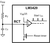 Figure 13. Off-timer Circuitry for Boost and Buck-boost Regulators
For a buck topology, RT and CT are also used to set tOFF, however the VIN proportionality will not ensure a constant switching frequency. Instead, constant ripple operation can be achieved. Changing the connection of RT in Figure 13 from VSW to VIN will provide a constant ripple over varying VIN. Adding a PNP transistor as shown in Figure 14 will provide constant ripple over varying VO.
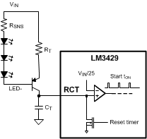 Figure 14. Off-timer Circuitry for Buck Regulators
The switching frequency is defined:
Buck (Constant Ripple vs. VIN)

Buck (Constant Ripple vs. VO)

Boost and Buck-Boost

For all topologies, the CT capacitor is recommended to be 1 nF and should be located very close to the LM3429.
7.3.4 Average LED Current
The LM3429 uses an external current sense resistor (RSNS) placed in series with the LED load to convert the LED current (ILED) into a voltage (VSNS) as shown in Figure 15. The HSP and HSN pins are the inputs to the high-side sense amplifier which are forced to be equal potential (VHSP=VHSN) through negative feedback. Because of this, the VSNS voltage is forced across RHSP to generate the signal current (ICSH) which flows out of the CSH pin and through the RCSH resistor. The error amplifier will regulate the CSH pin to 1.24 V, therefore ICSH can be calculated:

This means VSNS will be regulated as follows:

ILED can then be calculated:

The selection of the three resistors (RSNS, RCSH, and RHSP) is not arbitrary. For matching and noise performance, the suggested signal current ICSH is approximately 100 µA. This current does not flow in the LEDs and will not affect either the off state LED current or the regulated LED current. ICSH can be above or below this value, but the high-side amplifier offset characteristics may be affected slightly. In addition, to minimize the effect of the high-side amplifier voltage offset on LED current accuracy, the minimum VSNS is suggested to be 50 mV. Finally, a resistor (RHSN = RHSP) should be placed in series with the HSN pin to cancel out the effects of the input bias current (~10 µA) of both inputs of the high-side sense amplifier. The CSH pin can also be used as a low-side current sense input regulated to 1.24 V. The high-side sense amplifier is disabled if HSP and HSN are tied to GND.
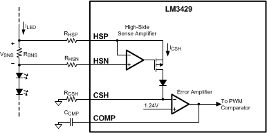 Figure 15. LED Current Sense Circuitry
7.3.5 Analog Dimming
The CSH pin can be used to analog dim the LED current by adjusting the current sense voltage (VSNS). There are several different methods to adjust VSNS using the CSH pin:
- External variable resistance : Adjust a potentiometer placed in series with RCSH to vary VSNS.
- External variable current source: Source current (0 µA to ICSH) into the CSH pin to adjust VSNS.
In general, analog dimming applications require a lower switching frequency to minimize the effect of the leading edge blanking circuit. As the LED current is reduced, the output voltage and the duty cycle decreases. Eventually, the minimum on-time is reached. The lower the switching frequency, the wider the linear dimming range. Figure 16 shows how both methods are physically implemented.
Method 1 uses an external potentiometer in the CSH path which is a simple addition to the existing circuitry. However, the LEDs cannot dim completely because there is always some resistance causing signal current to flow. This method is also susceptible to noise coupling at the CSH pin because the potentiometer increases the size of the signal current loop.
Method 2 provides a complete dimming range and better noise performance, though it is more complex. It consists of a PNP current mirror and a bias network consisting of an NPN, 2 resistors and a potentiometer (RADJ), where RADJ controls the amount of current sourced into the CSH pin. A higher resistance value will source more current into the CSH pin causing less regulated signal current through RHSP, effectively dimming the LEDs. VREF should be a precise external voltage reference, while Q7 and Q8 should be a dual pair PNP for best matching and performance. The additional current (IADD) sourced into the CSH pin can be calculated:

The corresponding ILED for a specific IADD is:

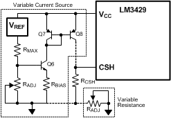 Figure 16. Analog Dimming Circuitry
7.3.6 Current Sense and Current Limit
The LM3429 achieves peak current mode control using a comparator that monitors the MosFET transistor current, comparing it with the COMP pin voltage as shown in Figure 17. Further, it incorporates a cycle-by-cycle overcurrent protection function. Current limit is accomplished by a redundant internal current sense comparator. If the voltage at the current sense comparator input (IS) exceeds 245 mV (typical), the on cycle is immediately terminated. The IS input pin has an internal N-channel MosFET which pulls it down at the conclusion of every cycle. The discharge device remains on an additional 250 ns (typical) after the beginning of a new cycle to blank the leading edge spike on the current sense signal. The leading edge blanking (LEB) determines the minimum achievable on-time (tON-MIN).
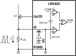 Figure 17. Current Sense / Current Limit Circuitry
There are two possible methods to sense the transistor current. The RDS-ON of the main power MosFET can be used as the current sense resistance because the IS pin was designed to withstand the high voltages present on the drain when the MosFET is in the off state. Alternatively, a sense resistor located in the source of the MosFET may be used for current sensing, however a low inductance (ESL) type is suggested. The cycle-by-cycle current limit (ILIM) can be calulated using either method as the limiting resistance (RLIM):

In general, the external series resistor allows for more design flexibility, however it is important to ensure all of the noise sensitive low power ground connections are connected together local to the controller and a single connection is made to the high current PGND (sense resistor ground point).
7.3.7 Control Loop Compensation
The LM3429 control loop is modeled like any current mode controller. Using a first order approximation, the uncompensated loop can be modeled as a single pole created by the output capacitor and, in the boost and buck-boost topologies, a right half plane zero created by the inductor, where both have a dependence on the LED string dynamic resistance. There is also a high frequency pole in the model, however it is above the switching frequency and plays no part in the compensation design process therefore it will be neglected. Because ceramic capacitance is recommended for use with LED drivers due to long lifetimes and high ripple current rating, the ESR of the output capacitor can also be neglected in the loop analysis. Finally, there is a DC gain of the uncompensated loop which is dependent on internal controller gains and the external sensing network.
A buck-boost regulator will be used as an example case. See the Typical Applications section for compensation of all topologies.
The uncompensated loop gain for a buck-boost regulator is given by the following equation:

Where the uncompensated DC loop gain of the system is described as:

And the output pole (ωP1) is approximated:

And the right half plane zero (ωZ1) is:

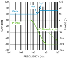 Figure 18. Uncompensated Loop Gain Frequency Response
Figure 18 shows the uncompensated loop gain in a worst-case scenario when the RHP zero is below the output pole. This occurs at high duty cycles when the regulator is trying to boost the output voltage significantly. The RHP zero adds 20dB/decade of gain while loosing 45°/decade of phase which places the crossover frequency (when the gain is zero dB) extremely high because the gain only starts falling again due to the high frequency pole (not modeled or shown in figure). The phase will be below -180° at the crossover frequency which means there is no phase margin (180° + phase at crossover frequency) causing system instability. Even if the output pole is below the RHP zero, the phase will still reach -180° before the crossover frequency in most cases yielding instability.
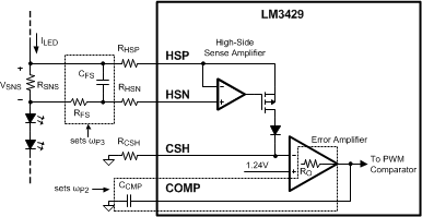 Figure 19. Compensation Circuitry
To mitigate this problem, a compensator should be designed to give adequate phase margin (above 45°) at the crossover frequency. A simple compensator using a single capacitor at the COMP pin (CCMP) will add a dominant pole to the system, which will ensure adequate phase margin if placed low enough. At high duty cycles (as shown in Figure 18), the RHP zero places extreme limits on the achievable bandwidth with this type of compensation. However, because an LED driver is essentially free of output transients (except catastrophic failures open or short), the dominant pole approach, even with reduced bandwidth, is usually the best approach. The dominant compensation pole (ωP2) is determined by CCMP and the output resistance (RO) of the error amplifier (typically 5 MΩ):

It may also be necessary to add one final pole at least one decade above the crossover frequency to attenuate switching noise and, in some cases, provide better gain margin. This pole can be placed across RSNS to filter the ESL of the sense resistor at the same time. Figure 19 shows how the compensation is physically implemented in the system.
The high frequency pole (ωP3) can be calculated:

The total system transfer function becomes:

The resulting compensated loop gain frequency response shown in Figure 20 indicates that the system has adequate phase margin (above 45°) if the dominant compensation pole is placed low enough, ensuring stability:
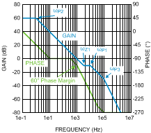 Figure 20. Compensated Loop Gain Frequency Response
7.3.8 Output Overvoltage Lockout (OVLO)
The LM3429 can be configured to detect an output (or input) overvoltage condition through the OVP pin. The pin features a precision 1.24-V threshold with 20 µA (typical) of hysteresis current as shown in Figure 21. When the OVLO threshold is exceeded, the GATE pin is immediately pulled low and a 20 µA current source provides hysteresis to the lower threshold of the OVLO hysteretic band.
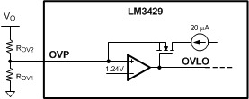 Figure 21. Overvoltage Protection Circuitry
If the LEDs are referenced to a potential other than ground (floating), as in the buck-boost and buck configuration, the output voltage (VO) should be sensed and translated to ground by using a single PNP as shown in Figure 22.
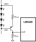 Figure 22. Floating Output OVP Circuitry
The overvoltage turnoff threshold (VTURN-OFF) is defined as follows:
Ground Referenced

Floating

In the ground referenced configuration, the voltage across ROV2 is VO - 1.24 V whereas in the floating configuration it is VO - 620 mV where 620 mV approximates the VBE of the PNP transistor.
The overvoltage hysteresis (VHYSO) is defined as follows:

7.3.9 Input Undervoltage Lockout (UVLO)
The nDIM pin is a dual-function input that features an accurate 1.24 V threshold with programmable hysteresis as shown in Figure 23. This pin functions as both the PWM dimming input for the LEDs and as a VIN UVLO. When the pin voltage rises and exceeds the 1.24 V threshold, 20 µA (typical) of current is driven out of the nDIM pin into the resistor divider providing programmable hysteresis.
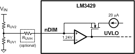 Figure 23. UVLO Circuit
When using the nDIM pin for UVLO and PWM dimming concurrently, the UVLO circuit can have an extra series resistor to set the hysteresis. This allows the standard resistor divider to have smaller resistor values minimizing PWM delays due to a pulldown MosFET at the nDIM pin (see PWM Dimming section). In general, at least 3V of hysteresis is necessary when PWM dimming if operating near the UVLO threshold.
The turn-on threshold (VTURN-ON) is defined as follows:

The hysteresis (VHYS) is defined as follows:
UVLO Only

PWM Dimming and UVLO

7.3.10 PWM Dimming
The active low nDIM pin can be driven with a PWM signal which controls the main NFET (Q1). The brightness of the LEDs can be varied by modulating the duty cycle of this signal. LED brightness is approximately proportional to the PWM signal duty cycle, so 30% duty cycle equals approximately 30% LED brightness. This function can be ignored if PWM dimming is not required by using nDIM solely as a VIN UVLO input as described in the Input Undervoltage Lockout (UVLO) section or by tying it directly to VCC or VIN (if less than 76VDC).
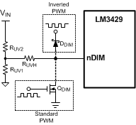 Figure 24. PWM Dimming Circuit
Figure 24 shows two ways the PWM signal can be applied to the nDIM pin:
- Connect the dimming MosFET (QDIM) with the drain to the nDIM pin and the source to GND. Apply an external logic-level PWM signal to the gate of QDIM. A pull down resistor may be necessary to properly turn off QDIM if no signal is present.
- Connect the anode of a Schottky diode (DDIM) to the nDIM pin. Apply an external inverted logic-level PWM signal to the cathode of the same diode.
A minimum on-time must be maintained in order for PWM dimming to operate in the linear region of its transfer function. Because the controller is disabled during dimming, the PWM pulse must be long enough such that the energy intercepted from the input is greater than or equal to the energy being put into the LEDs. For boost and buck-boost regulators, the following condition must be maintained:

In the previous equation, tPULSE is the length of the PWM pulse in seconds.
7.3.11 Startup Regulator (VCC LDO)
The LM3429 includes a high voltage, low dropout (LDO) bias regulator. When power is applied, the regulator is enabled and sources current into an external capacitor connected to the VCC pin. The VCC output voltage is 6.9V nominally and the supply is internally current limited to 20 mA (minimum). The recommended bypass capacitance range for the VCC regulator is 2.2 µF to 3.3 µF. The output of the VCC regulator is monitored by an internal UVLO circuit that protects the device during startup, normal operation, and shutdown from attempting to operate with insufficient supply voltage.
7.3.12 Thermal Shutdown
The LM3429 includes thermal shutdown. If the die temperature reaches approximately 165°C the device will shut down (GATE pin low), until it reaches approximately 140°C where it turns on again.
7.4 Device Functional Modes
This device has no functional modes.