SNVS682D November 2010 – December 2015 LM3444
PRODUCTION DATA.
- 1 Features
- 2 Applications
- 3 Description
- 4 Revision History
- 5 Pin Configuration and Functions
- 6 Specifications
- 7 Detailed Description
-
8 Application and Implementation
- 8.1
Application Information
- 8.1.1 Determining Duty-Cycle (D)
- 8.1.2 Calculating Off-Time
- 8.1.3 Setting the Switching Frequency
- 8.1.4 Inductor Selection
- 8.1.5 Setting the LED Current
- 8.1.6 Valley Fill Capacitors
- 8.1.7 Determining the Capacitance Value of the Valley-Fill Capacitors
- 8.1.8 Determining Maximum Number of Series Connected LEDs Allowed
- 8.1.9 Output Capacitor
- 8.1.10 Switching MOSFET
- 8.1.11 Recirculating Diode
- 8.2 Typical Application
- 8.1
Application Information
- 9 Power Supply Recommendations
- 10Layout
- 11Device and Documentation Support
Package Options
Mechanical Data (Package|Pins)
Thermal pad, mechanical data (Package|Pins)
Orderable Information
7 Detailed Description
7.1 Overview
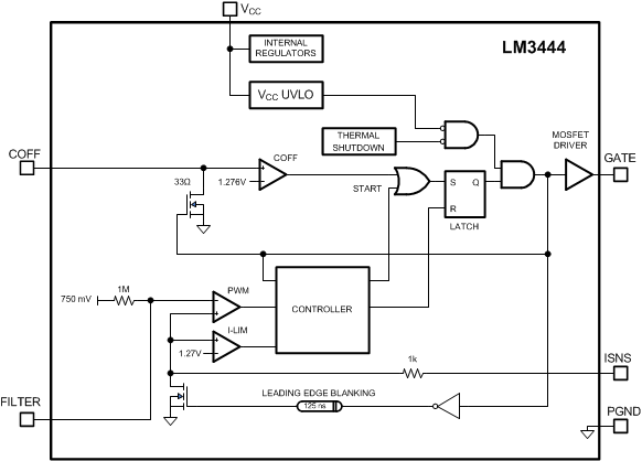
The LM3444 device contains all the necessary circuitry to build a line-powered (mains powered) constant current LED driver.
7.2 Functional Block Diagram
7.3 Feature Description
7.3.1 Theory of Operation
For an image of the LM3444 along with basic external circuitry, see Figure 8.
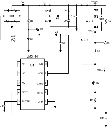 Figure 8. LM3444 Schematic
7.3.2 Valley-Fill Circuit
VBUCK supplies the power which drives the LED string. Diode D3 allows VBUCK to remain high while V+ cycles on and off. VBUCK has a relatively small hold capacitor C10 which reduces the voltage ripple when the valley fill capacitors are being charged. However, the network of diodes and capacitors shown between D3 and C10 make up a valley-fill circuit. The valley-fill circuit can be configured with two or three stages. The most common configuration is two stages. Figure 9 illustrates a two- and three-stage valley-fill circuit.
 Figure 9. Two and Three Stage Valley Fill Circuit
The valley-fill circuit allows the buck regulator to draw power throughout a larger portion of the AC line. This allows the capacitance needed at VBUCK to be lower than if there were no valley-fill circuit, and adds passive power factor correction (PFC) to the application.
7.3.3 Valley-Fill Operation
When the input line is high, power is derived directly through D3. The term input line is high is explained as follows. The valley-fill circuit charges capacitors C7 and C9 in series (Figure 10) when the input line is high.
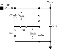 Figure 10. Two Stage Valley-Fill Circuit When AC Line is High
The peak voltage of a two-stage valley-fill capacitor is given by Equation 1.

As the AC line decreases from its peak value every cycle, there is a point where the voltage magnitude of the AC line is equal to the voltage that each capacitor is charged. At this point, diode D3 becomes reversed biased, and the capacitors are placed in parallel to each other (Figure 11), and VBUCK equals the capacitor voltage.
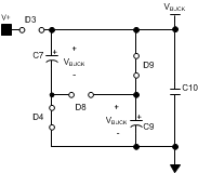 Figure 11. Two Stage Valley-Fill Circuit when AC Line is Low
A three stage valley-fill circuit performs exactly the same as two-stage valley-fill circuit, except now three capacitors are charged in series when the line voltage decreases, as shown in Equation 2:

Diode D3 is reverse-biased and three capacitors are in parallel to each other.
The valley-fill circuit can be optimized for power factor, voltage hold-up, and overall application size and cost. The LM3444 operates with a single-stage or a three-stage valley-fill circuit as well. Resistor R8 functions as a current limiting resistor during start-up, and during the transition from series to parallel connection. Resistors R6 and R7 are 1-MΩ bleeder resistors, and may or may not be necessary for each application.
7.3.4 Buck Converter
The LM3444 is a buck controller that uses a proprietary constant off-time method to maintain constant current through a string of LEDs. While transistor Q2 is on, current ramps up through the inductor and LED string. A resistor R3 senses this current and this voltage is compared to the reference voltage at FILTER. When this sensed voltage is equal to the reference voltage, transistor Q2 is turned off and diode D10 conducts the current through the inductor and LEDs. Capacitor C12 eliminates most of the ripple current seen in the inductor. Resistor R4, capacitor C11, and transistor Q3 provide a linear current ramp that sets the constant off-time for a given output voltage.
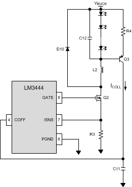 Figure 12. LM3444 Buck Regulation Circuit
7.3.5 Overview Of Constant Off-Time Control
The conversion ratio of a buck converter is defined as given by Equation 3.

Constant off-time control architecture operates by simply defining the off-time and allowing the on-time, and therefore the switching frequency, to vary as either VIN or VO changes. The output voltage is equal to the LED string voltage (VLED), and should not change significantly for a given application. The input voltage or VBUCK in this analysis varies as the input line varies. The length of the on-time is determined by the sensed inductor current through a resistor to a voltage reference at a comparator. During the on-time, denoted by tON, MOSFET switch Q2 is on causing the inductor current to increase. During the on-time, current flows from VBUCK, through the LEDs, through L2, Q2, and finally through R3 to ground. At some point in time, the inductor current reaches a maximum (IL2-PK) determined by the voltage sensed at R3 and the ISNS pin. This sensed voltage across R3 is compared against the voltage of FILTER, at which point Q2 is turned off by the controller.
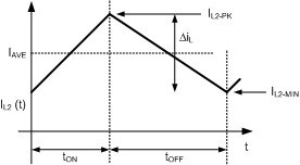 Figure 13. Inductor Current Waveform in CCM
During the off-period denoted by tOFF, the current through L2 continues to flow through the LEDs through D10.
7.3.6 Thermal Shutdown
Thermal shutdown limits total power dissipation by turning off the output switch when the IC junction temperature exceeds 165°C. After thermal shutdown occurs, the output switch does not turn on until the junction temperature drops to approximately 145°C.
7.4 Device Functional Modes
This device does not have any additional functional modes.