SNVS682D November 2010 – December 2015 LM3444
PRODUCTION DATA.
- 1 Features
- 2 Applications
- 3 Description
- 4 Revision History
- 5 Pin Configuration and Functions
- 6 Specifications
- 7 Detailed Description
-
8 Application and Implementation
- 8.1
Application Information
- 8.1.1 Determining Duty-Cycle (D)
- 8.1.2 Calculating Off-Time
- 8.1.3 Setting the Switching Frequency
- 8.1.4 Inductor Selection
- 8.1.5 Setting the LED Current
- 8.1.6 Valley Fill Capacitors
- 8.1.7 Determining the Capacitance Value of the Valley-Fill Capacitors
- 8.1.8 Determining Maximum Number of Series Connected LEDs Allowed
- 8.1.9 Output Capacitor
- 8.1.10 Switching MOSFET
- 8.1.11 Recirculating Diode
- 8.2 Typical Application
- 8.1
Application Information
- 9 Power Supply Recommendations
- 10Layout
- 11Device and Documentation Support
Package Options
Mechanical Data (Package|Pins)
Thermal pad, mechanical data (Package|Pins)
Orderable Information
10 Layout
10.1 Layout Guidelines
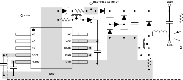
Keep the low power components for FILTER and COFF close to the LM3444 with short traces. The ISNS trace should also be as short and direct as possible. Keep the high current switching paths generated by R3, Q2, L2, and D10 as short as possible to minimize generated switching noise and improve EMI.
10.2 Layout Example
 Figure 21. Layout Recommendation