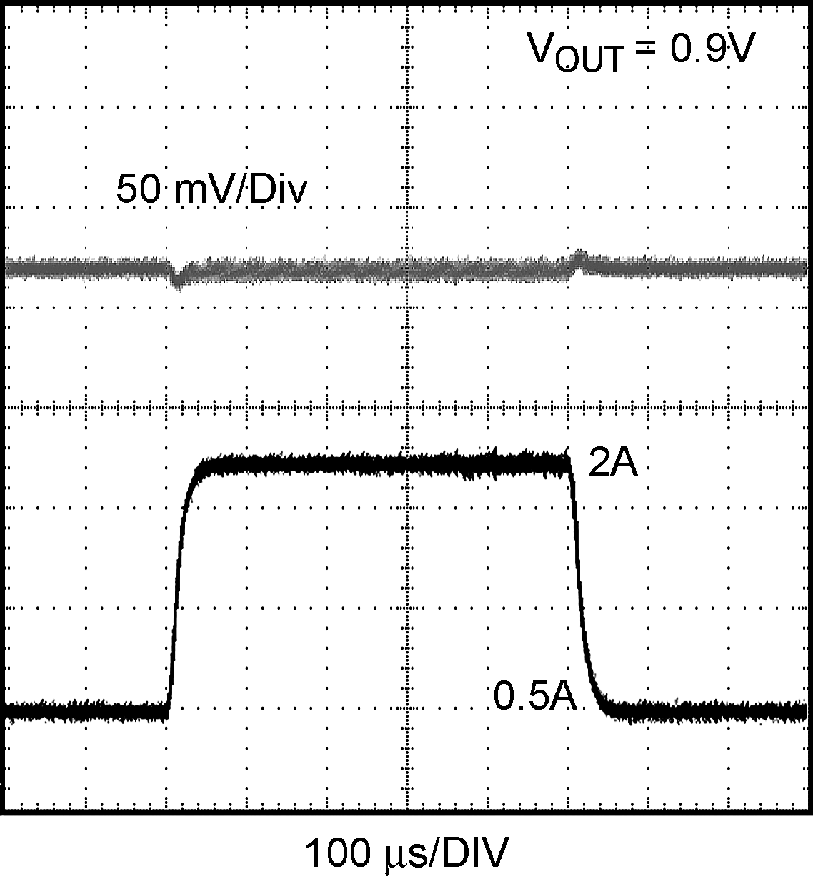
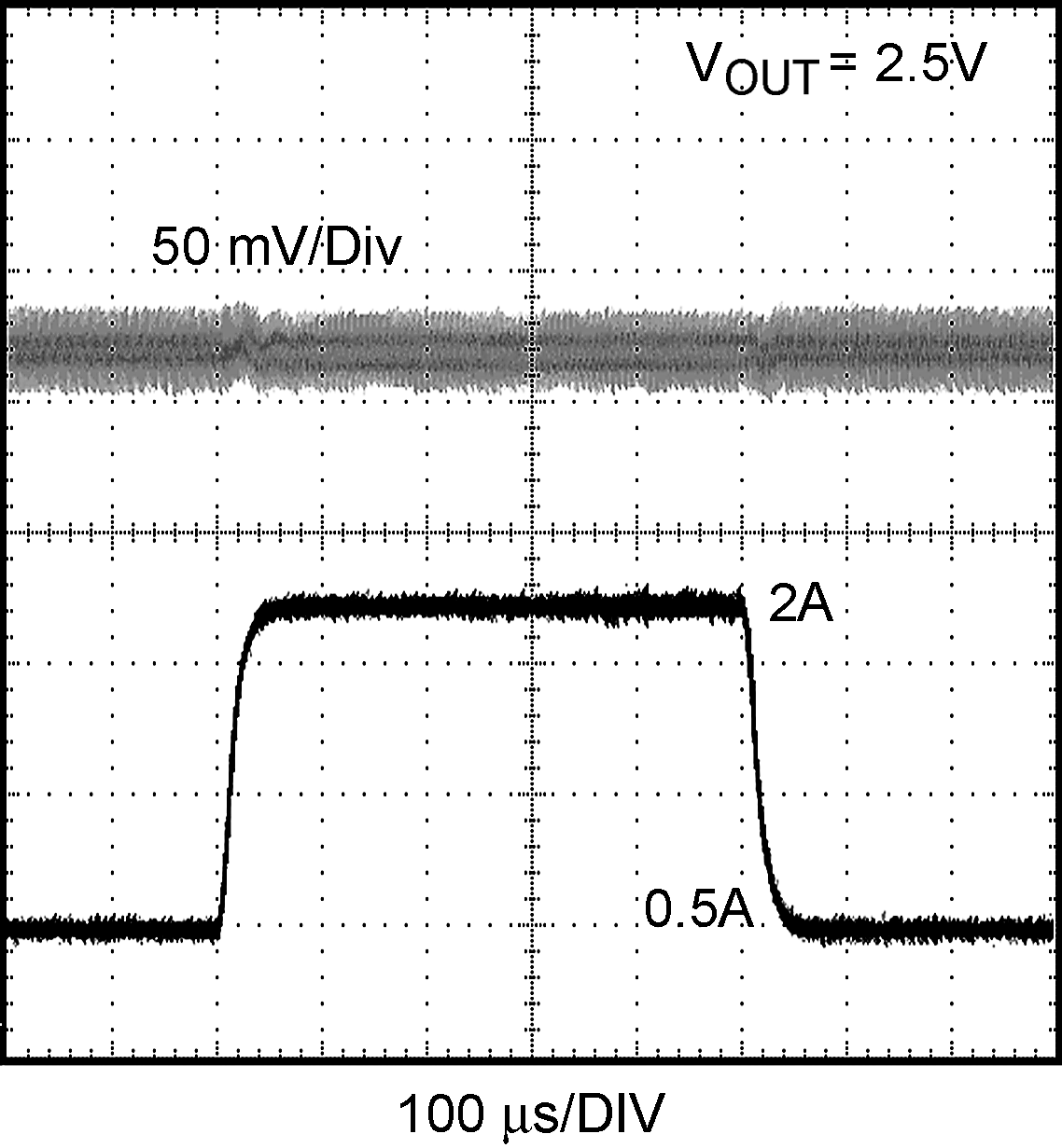
SNVS239C October 2004 – October 2015 LM3475
PRODUCTION DATA.
- 1 Features
- 2 Applications
- 3 Description
- 4 Revision History
- 5 Pin Configuration and Functions
- 6 Specifications
- 7 Detailed Description
-
8 Application and Implementation
- 8.1 Application Information
- 8.2
Typical Application
- 8.2.1 Design Requirements
- 8.2.2
Detailed Design Procedure
- 8.2.2.1 Setting Output Voltage
- 8.2.2.2 Setting Operating Frequency and Output Ripple
- 8.2.2.3 Using a Feed-forward Capacitor
- 8.2.2.4 Inductor Selection
- 8.2.2.5 Output Capacitor Selection
- 8.2.2.6 Input Capacitor Selection
- 8.2.2.7 Diode Selection
- 8.2.2.8 P-Channel MOSFET Selection
- 8.2.2.9 Reducing Switching Noise
- 8.2.3 Application Curves
- 9 Power Supply Recommendations
- 10Layout
- 11Device and Documentation Support
- 12Mechanical, Packaging, and Orderable Information
Package Options
Mechanical Data (Package|Pins)
- DBV|5
Thermal pad, mechanical data (Package|Pins)
Orderable Information
8 Application and Implementation
NOTE
Information in the following applications sections is not part of the TI component specification, and TI does not warrant its accuracy or completeness. TI’s customers are responsible for determining suitability of components for their purposes. Customers should validate and test their design implementation to confirm system functionality.
8.1 Application Information
The LM3475 employs a hysteretic control architecture; which provides excellent load transient response and efficiency even at light loads, as compared to its PWM architectures. No external compensation is required which results in a simple design and low component count. A typical schematic is described in the next section.
8.2 Typical Application
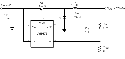 Figure 10. Full Demo Board Schematic
8.2.1 Design Requirements
To properly size the components for the application, the designer needs the following parameters: input voltage range, output voltage, output current range, and required switching frequency. These four main parameters affect the choices of component available to achieve a proper system behavior. Although hysteretic control is a simple control scheme, the operating frequency and other performance characteristics depend on external conditions and components. If the inductance, output capacitance, ESR, VIN, or Cff is changed, there will be a change in the operating frequency and possibly output ripple. Therefore, care must be taken to select components which will provide the desired operating range.
8.2.2 Detailed Design Procedure
Table 1. Bill of Materials
| DESIGNATOR | DESCRIPTION | PART NUMBER | VENDOR |
|---|---|---|---|
| CIN | 10 µF, 16 V, X5R | EMK325BJ106MN | TAIYO YUDEN |
| COUT | 100 µF, 6 V, Ta | TPSY107M006R0100 | AVX |
| CFF | 1 nF, 25 V, X7R | VJ1206Y102KXXA | Vishay |
| D1 | Schottky, 20 V, 2 A | CMSH2-20L | Central Semiconductor |
| L1 | 10 µH, 3.1 A | CDRH103R100 | Sumida |
| Q1 | 30 V, 2.5 A | Si2343 | Vishay |
| RFB2 | 1 kΩ, 0805, 1% | CRW08051001F | Vishay |
| RFB1 | 2.15 kΩ, 0805, 1% | CRCW08052151F | Vishay |
8.2.2.1 Setting Output Voltage
The output voltage is programmed using a resistor divider between VOUT and GND as shown in Figure 11. The feedback resistors can be calculated as follows:

where
- Vfb is 0.8 V typically
The feedback resistor ratio, α = (R1+R2) / R2, will also be used below to calculate output ripple and operating frequency.
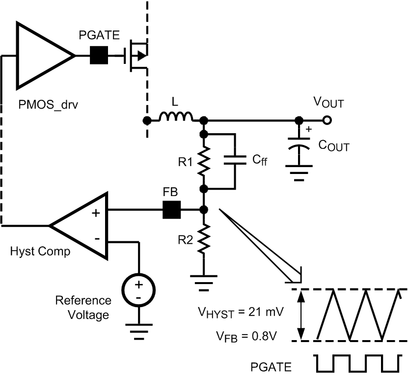 Figure 11. Hysteretic Window
8.2.2.2 Setting Operating Frequency and Output Ripple
Although hysteretic control is a simple control scheme, the operating frequency and other performance characteristics depend on external conditions and components. If the inductance, output capacitance, ESR, VIN, or Cff is changed, there will be a change in the operating frequency and possibly output ripple. Therefore, care must be taken to select components which will provide the desired operating range. The best approach is to determine what operating frequency is desirable in the application and then begin with the selection of the inductor and output capacitor ESR. The design process usually involves a few iterations to select appropriate standard values that will result in the desired frequency and ripple.
Without the feedforward capacitor (Cff), the operating frequency (F) can be approximately calculated using the formula:

where
- Delay is the sum of the LM3475 propagation delay time and the PFET delay time
- The propagation delay is 90ns typically
Minimum output ripple voltage can be determined using the following equation:
8.2.2.3 Using a Feed-forward Capacitor
The operating frequency and output ripple voltage can also be significantly influenced using a speed up capacitor, Cff, as shown in Figure 11. Cff is connected in parallel with the high side feedback resistor, R1. The output ripple causes a current to be sourced or sunk through this capacitor. This current is essentially a square wave. Since the input to the feedback pin (FB) is a high impedance node, the bulk of the current flows through R2. This superimposes a square wave ripple voltage on the FB node. The end result is a reduction in output ripple and an increase in operating frequency. When adding Cff, calculate the formula above with α= 1. The value of Cff depends on the desired operating frequency and the value of R2. A good starting point is 1nF ceramic at 100kHz decreasing linearly with increased operating frequency. Also note that as the output voltage is programmed below 1.6V, the effect of Cff will decrease significantly.
8.2.2.4 Inductor Selection
The most important parameters for the inductor are the inductance and the current rating. The LM3475 operates over a wide frequency range and can use a wide range of inductance values. Minimum inductance can be calculated using the following equation:

where
- D is the duty cycle, defined as VOUT/VIN
- ΔI is the allowable inductor ripple current
Maximum allowable inductor ripple current should be calculated as a function of output current (IOUT) as shown below:
ΔImax = IOUT x 0.3
The inductor must also be rated to handle the peak current (IPK) and RMS current given by:

The inductance value and the resulting ripple is one of the key parameters controlling operating frequency.
8.2.2.5 Output Capacitor Selection
Once the desired operating frequency and inductance value are selected, ESR must be selected based on Equation 4. This process may involve a few iterations to select standard ESR and inductance values.
In general, the ESR of the output capacitor and the inductor ripple current create the output ripple of the regulator. However, the comparator hysteresis sets the first order value of this ripple. Therefore, as ESR and ripple current vary, operating frequency must also vary to keep the output ripple voltage regulated. The hysteretic control topology is well suited to using ceramic output capacitors. However, ceramic capacitors have a very low ESR, resulting in a 90° phase shift of the output voltage ripple. This results in low operating frequency and increased output ripple. To fix this problem a low value resistor could be added in series with the ceramic output capacitor. Although counter intuitive, this combination of a ceramic capacitor and external series resistance provide highly accurate control over the output voltage ripple. Another method is to add an external ramp at the FB pin as shown in Figure 12. By proper selection of R1 and C2, the FB pin sees faster voltage change than the output ripple can cause. As a result, the switching frequency is higher while the output ripple becomes lower. The switching frequency is approximately:

Other types of capacitor, such as Sanyo POSCAP, OS-CON, and Nichicon ’NA’ series are also recommended and may be used without additional series resistance. For all practical purposes, any type of output capacitor may be used with proper circuit verification.
Capacitors with high ESL (equivalent series inductance) values should not be used. As shown in Figure 9, the output ripple voltage contains a small step at both the high and low peaks. This step is caused by and is directly proportional to the output capacitor’s ESL. A large ESL, such as in an electrolytic capacitor, can create a step large enough to cause abnormal switching behavior.
8.2.2.6 Input Capacitor Selection
A bypass capacitor is required between VIN and ground. It must be placed near the source of the external PFET. The input capacitor prevents large voltage transients at the input and provides the instantaneous current when the PFET turns on. The important parameters for the input capacitor are the voltage rating and the RMS current rating. Follow the manufacturer’s recommended voltage de-rating. RMS current and power dissipation (PD) can be calculated with the equations below:

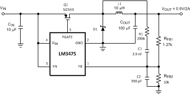 Figure 12. External Ramp
8.2.2.7 Diode Selection
The catch diode provides the current path to the load during the PFET off time. Therefore, the current rating of the diode must be higher than the average current through the diode, which be calculated as shown:
The peak voltage across the catch diode is approximately equal to the input voltage. Therefore, the diode’s peak reverse voltage rating should be greater than 1.3 times the input voltage.
A Schottky diode is recommended, since a low forward voltage drop will improve efficiency.
For high temperature applications, diode leakage current may become significant and require a higher reverse voltage rating to achieve acceptable performance.
8.2.2.8 P-Channel MOSFET Selection
The PFET switch should be selected based on the maximum Drain-Source voltage (VDS), Drain current rating (ID), maximum Gate-Source voltage (VGS), on resistance (RDSON), and Gate capacitance. The voltage across the PFET when it is turned off is equal to the sum of the input voltage and the diode forward voltage. The VDS must be selected to provide some margin beyond the sum of the input voltage and Vd.
Since the current flowing through the PFET is equal to the current through the inductor, ID must be rated higher than the maximum IPK. During switching, PGATE swings the PFET’s gate from VIN to ground. Therefore, A PFET must be selected with a maximum VGS larger than VIN. To insure that the PFET turns on completely and quickly, refer to the PGATE section.
The power loss in the PFET consists of switching losses and conducting losses. Although switching losses are difficult to precisely calculate, the equation below can be used to estimate total power dissipation. Increasing RDSON will increase power losses and degrade efficiency. Note that switching losses will also increase with lower gate threshold voltages.
where
- ton = FET turn on time
- toff = FET turn off time
- A value of 10ns to 50ns is typical for ton and toff
Note that the RDSON has a positive temperature coefficient. At 100°C, the RDSON may be as much as 150% higher than the value at 25°C.
The Gate capacitance of the PFET has a direct impact on both PFET transition time and the power dissipation in the LM3475. Most of the power dissipated in the LM3475 is used to drive the PFET switch. This power can be calculated as follows:
The amount of average gate driver current required during switching (IG) is:
And the total power dissipated in the device is:
where
- Iq is typically 260µA as shown in Electrical Characteristics
As gate capacitance increases, operating frequency may need to be reduced, or additional heat sinking may be required to lower the power dissipation in the device.
In general, keeping the gate capacitance below 2000 pF is recommended to keep transition times (switching losses), and power losses low.
8.2.2.9 Reducing Switching Noise
Although the LM3475 employs internal noise suppression circuitry, external noise may continue to be excessive. There are several methods available to reduce noise and EMI.
MOSFETs are very fast switching devices. The fast increase in PFET current coupled with parasitic trace inductance can create unwanted noise spikes at both the switch node and at VIN. Switching noise will increase with load current and input voltage. This noise can also propagate through the ground plane, sometimes causing unpredictable device performance. Slowing the rise and fall times of the PFET can be very effective in reducing this noise. Referring to Figure 13, the PFET can be slowed down by placing a small (1-Ω to 10-Ω) resistor in series with PGATE. However, this resistor will increase the switching losses in the PFET and will lower efficiency. Therefore it should be kept as small as possible and only used when necessary. Another method to reduce switching noise (other than good PCB layout, see Layout) is to use a small RC filter or snubber. The snubber should be placed in parallel with the catch diode, connected close to the drain of the PFET, as shown in Figure 13. Again, the snubber should be kept as small as possible to limit its impact on system efficiency. A typical range is a 10-Ω to 100-Ω resistor and a 470-pF to 2.2-nF ceramic capacitor.
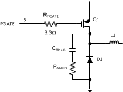 Figure 13. PGATE Resistor and Snubber
