SNVS085X July 2000 – December 2017 LM3478
PRODUCTION DATA.
- 1 Features
- 2 Applications
- 3 Description
- 4 Revision History
- 5 Pin Configuration and Functions
- 6 Specifications
- 7 Detailed Description
-
8 Application and Implementation
- 8.1 Application Information
- 8.2
Typical Applications
- 8.2.1
Typical High Efficiency Step-Up (Boost) Converter
- 8.2.1.1 Design Requirements
- 8.2.1.2
Detailed Design Procedure
- 8.2.1.2.1 Custom Design with WEBENCH Tools
- 8.2.1.2.2 Power Inductor Selection
- 8.2.1.2.3 Programming the Output Voltage
- 8.2.1.2.4 Setting the Current Limit
- 8.2.1.2.5 Current Limit with External Slope Compensation
- 8.2.1.2.6 Power Diode Selection
- 8.2.1.2.7 Power MOSFET Selection
- 8.2.1.2.8 Input Capacitor Selection
- 8.2.1.2.9 Output Capacitor Selection
- 8.2.1.2.10 Compensation
- 8.2.1.3 Application Curves
- 8.2.2 Typical SEPIC Converter
- 8.2.1
Typical High Efficiency Step-Up (Boost) Converter
- 9 Power Supply Recommendations
- 10Layout
- 11Device and Documentation Support
- 12Mechanical, Packaging, and Orderable Information
Package Options
Mechanical Data (Package|Pins)
Thermal pad, mechanical data (Package|Pins)
Orderable Information
8.2.2.2.3 Selection of Inductors L1 and L2
Proper selection of inductors L1 and L2 to maintain continuous current conduction mode requires calculations of the following parameters.
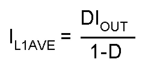
Average current in the inductors can be calculated using Equation 39.

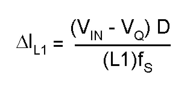
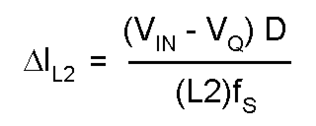
Peak to peak ripple current, to calculate core loss if necessary using Equation 41 and Equation 42.


Maintaining the condition IL > ΔiL/2 to ensure continuous current conduction yields Equation 43 and Equation 44.


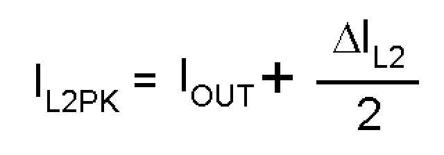
Peak current in the inductor, use Equation 45 and Equation 46 to ensure the inductor does not saturate.


IL1PK must be lower than the maximum current rating set by the current sense resistor.
The value of L1 can be increased above the minimum recommended to reduce input ripple and output ripple. However, once DIL1 is less than 20% of IL1AVE, the benefit to output ripple is minimal.
By increasing the value of L2 above the minimum recommended, ΔIL2 can be reduced, which in turn will reduce the output ripple voltage:

where ESR is the effective series resistance of the output capacitor.
If L1 and L2 are wound on the same core, then L1 = L2 = L. All of the previous equations will hold true if the inductance is replaced by 2L.