SNVS085X July 2000 – December 2017 LM3478
PRODUCTION DATA.
- 1 Features
- 2 Applications
- 3 Description
- 4 Revision History
- 5 Pin Configuration and Functions
- 6 Specifications
- 7 Detailed Description
-
8 Application and Implementation
- 8.1 Application Information
- 8.2
Typical Applications
- 8.2.1
Typical High Efficiency Step-Up (Boost) Converter
- 8.2.1.1 Design Requirements
- 8.2.1.2
Detailed Design Procedure
- 8.2.1.2.1 Custom Design with WEBENCH Tools
- 8.2.1.2.2 Power Inductor Selection
- 8.2.1.2.3 Programming the Output Voltage
- 8.2.1.2.4 Setting the Current Limit
- 8.2.1.2.5 Current Limit with External Slope Compensation
- 8.2.1.2.6 Power Diode Selection
- 8.2.1.2.7 Power MOSFET Selection
- 8.2.1.2.8 Input Capacitor Selection
- 8.2.1.2.9 Output Capacitor Selection
- 8.2.1.2.10 Compensation
- 8.2.1.3 Application Curves
- 8.2.2 Typical SEPIC Converter
- 8.2.1
Typical High Efficiency Step-Up (Boost) Converter
- 9 Power Supply Recommendations
- 10Layout
- 11Device and Documentation Support
- 12Mechanical, Packaging, and Orderable Information
Package Options
Mechanical Data (Package|Pins)
Thermal pad, mechanical data (Package|Pins)
Orderable Information
8.2.1.2.4 Setting the Current Limit
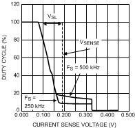
The maximum amount of current that can be delivered to the load is set by the sense resistor, RSEN. Current limit occurs when the voltage that is generated across the sense resistor equals the current sense threshold voltage, VSENSE. When this threshold is reached, the switch will be turned off until the next cycle. Limits for VSENSE are specified in the electrical characteristics section. VSENSE represents the maximum value of the internal control signal VCS as shown in Figure 30. This control signal, however, is not a constant value and changes over the course of a period as a result of the internal compensation ramp (VSL). Therefore the current limit threshold will also change. The actual current limit threshold is a function of the sense voltage (VSENSE) and the internal compensation ramp:
Where ISWLIMIT is the peak switch current limit, defined by Equation 17.
 Figure 30. Current Sense Voltage vs Duty Cycle
Figure 30 shows how VCS (and current limit threshold voltage) change with duty cycle. The curve is equivalent to the internal compensation ramp slope (Se) and is bounded at low duty cycle by VSENSE, shown as a dotted line. As duty cycle increases, the control voltage is reduced as VSL ramps up. The graph also shows the short circuit current limit threshold of 343 mV (typical) during the 325 ns (typical) blanking time. For higher frequencies this fixed blanking time obviously occupies more duty cycle, percentage wise. Since current limit threshold varies with duty cycle, the use Equation 17 to select RSEN and set the desired current limit threshold:

The numerator of Equation 17 is VCS, and ISWLIMIT using Equation 18.

To avoid false triggering, the current limit value should have some margin above the maximum operating value, typically 120%. Values for both VSENSE and VSL are specified in Electrical Characteristics. However, calculating with the limits of these two specs could result in an unrealistically wide current limit or RSEN range. Therefore, Equation 19 is recommended, using the VSL ratio value given in Electrical Characteristics.

RSEN is part of the current mode control loop and has some influence on control loop stability. Therefore, once the current limit threshold is set, loop stability must be verified. As described in the slope compensation section, Equation 20 must hold true for a current mode converter to be stable.
To verify that this equation holds true, use Equation 21.

If the selected RSEN is greater than this value, additional slope compensation must be added to ensure stability, as described in the section below.