SNVSCL9B March 2011 – December 2024 LM3481-Q1
PRODUCTION DATA
- 1
- 1 Features
- 2 Applications
- 3 Description
- 4 Pin Configuration and Functions
- 5 Specifications
- 6 Detailed Description
-
7 Application and Implementation
- 7.1 Application Information
- 7.2
Typical Applications
- 7.2.1
Boost Converter
- 7.2.1.1 Design Requirements
- 7.2.1.2
Detailed Design Procedure
- 7.2.1.2.1 Custom Design with WEBENCH Tools
- 7.2.1.2.2 Power Inductor Selection
- 7.2.1.2.3 Programming the Output Voltage and Output Current
- 7.2.1.2.4 Current Limit With Additional Slope Compensation
- 7.2.1.2.5 Power Diode Selection
- 7.2.1.2.6 Power MOSFET Selection
- 7.2.1.2.7 Input Capacitor Selection
- 7.2.1.2.8 Output Capacitor Selection
- 7.2.1.2.9 Driver Supply Capacitor Selection
- 7.2.1.2.10 Compensation
- 7.2.1.3 Application Curve
- 7.2.2 Typical SEPIC Converter
- 7.2.1
Boost Converter
- 7.3 Power Supply Recommendations
- 7.4 Layout
- 8 Device and Documentation Support
- 9 Revision History
- 10Mechanical, Packaging, and Orderable Information
Package Options
Mechanical Data (Package|Pins)
- DGS|10
Thermal pad, mechanical data (Package|Pins)
Orderable Information
6.1 Overview
The LM3481-Q1 device uses a fixed frequency, Pulse Width Modulated (PWM), current mode control architecture. In a typical application circuit, the peak current through the external MOSFET is sensed through an external sense resistor. The voltage across this resistor is fed into the ISEN pin. This voltage is then level shifted and fed into the positive input of the PWM comparator. The output voltage is also sensed through an external feedback resistor divider network and fed into the error amplifier (EA) negative input (feedback pin, FB). The output of the error amplifier (COMP pin) is added to the slope compensation ramp and fed into the negative input of the PWM comparator.
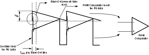
At the start of any switching cycle, the oscillator sets the RS latch using the SET/Blank-out and switch logic blocks. This forces a high signal on the DR pin (gate of the external MOSFET) and the external MOSFET turns on. When the voltage on the positive input of the PWM comparator exceeds the negative input, the RS latch is reset and the external MOSFET turns off.
The voltage sensed across the sense resistor generally contains spurious noise spikes, as shown in Figure 6-1. These spikes can force the PWM comparator to reset the RS latch prematurely. To prevent these spikes from resetting the latch, a blank-out circuit inside the IC prevents the PWM comparator from resetting the latch for a short duration after the latch is set. This duration, called the blank-out time, is typically 250 ns and is specified as tmin (on) in the Section 5.5 section.
Under extremely light load or no-load conditions, the energy delivered to the output capacitor when the external MOSFET is on during the blank-out time is more than what is delivered to the load. An overvoltage comparator inside the LM3481-Q1 prevents the output voltage from rising under these conditions by sensing the feedback (FB pin) voltage and resetting the RS latch. The latch remains in a reset state until the output decays to the nominal value. Thus the operating frequency decreases at light loads, resulting in excellent efficiency.
 Figure 6-1 Basic Operation of the PWM Comparator