SNVS346H November 2007 – October 2024 LM3481
PRODUCTION DATA
- 1
- 1 Features
- 2 Applications
- 3 Description
- 4 Pin Configuration and Functions
- 5 Specifications
- 6 Detailed Description
-
7 Application and Implementation
- 7.1 Application Information
- 7.2
Typical Applications
- 7.2.1
Boost Converter
- 7.2.1.1 Design Requirements
- 7.2.1.2
Detailed Design Procedure
- 7.2.1.2.1 Custom Design with WEBENCH Tools
- 7.2.1.2.2 Power Inductor Selection
- 7.2.1.2.3 Programming the Output Voltage and Output Current
- 7.2.1.2.4 Current Limit With Additional Slope Compensation
- 7.2.1.2.5 Power Diode Selection
- 7.2.1.2.6 Power MOSFET Selection
- 7.2.1.2.7 Input Capacitor Selection
- 7.2.1.2.8 Output Capacitor Selection
- 7.2.1.2.9 Driver Supply Capacitor Selection
- 7.2.1.2.10 Compensation
- 7.2.1.3 Application Curve
- 7.2.2 Typical SEPIC Converter
- 7.2.1
Boost Converter
- 7.3 Power Supply Recommendations
- 7.4 Layout
- 8 Device and Documentation Support
- 9 Revision History
- 10Mechanical, Packaging, and Orderable Information
Package Options
Mechanical Data (Package|Pins)
- DGS|10
Thermal pad, mechanical data (Package|Pins)
Orderable Information
7.2.2.2.3 Selection of Inductors L1 and L2
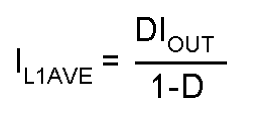
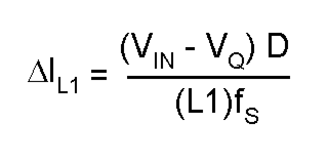
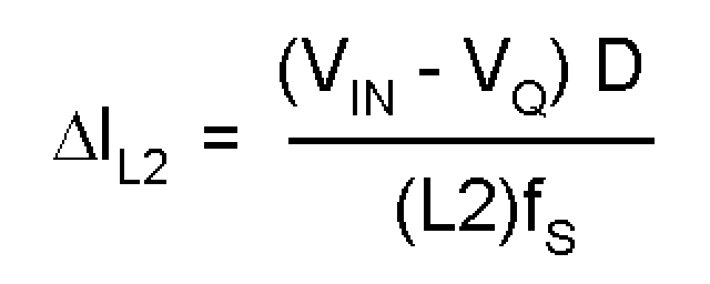
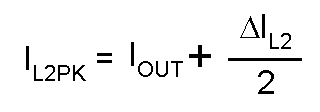
Proper selection of the inductors L1 and L2 to maintain constant current mode requires calculations of the following parameters.
Average current in the inductors:

Peak-to-peak ripple current, to calculate core loss if necessary:


Maintaining the condition IL > ΔIL/2 to ensure continuous conduction mode yields the following minimum values for L1 and L2:


Peak current in the inductor, to ensure the inductor does not saturate:


IL1PK must be lower than the maximum current rating set by the current sense resistor.
The value of L1 can be increased above the minimum recommended value to reduce input ripple and output ripple. However, once ΔIL1 is less than 20% of IL1AVE, the benefit to output ripple is minimal.
By increasing the value of L2 above the minimum recommendation, ΔIL2 can be reduced, which in turn will reduce the output ripple voltage:

where ESR is the effective series resistance of the output capacitor.
If L1 and L2 are wound on the same core, then L1 = L2 = L. All the equations above will hold true if the inductance is replaced by 2L.