SNVS346H November 2007 – October 2024 LM3481
PRODUCTION DATA
- 1
- 1 Features
- 2 Applications
- 3 Description
- 4 Pin Configuration and Functions
- 5 Specifications
- 6 Detailed Description
-
7 Application and Implementation
- 7.1 Application Information
- 7.2
Typical Applications
- 7.2.1
Boost Converter
- 7.2.1.1 Design Requirements
- 7.2.1.2
Detailed Design Procedure
- 7.2.1.2.1 Custom Design with WEBENCH Tools
- 7.2.1.2.2 Power Inductor Selection
- 7.2.1.2.3 Programming the Output Voltage and Output Current
- 7.2.1.2.4 Current Limit With Additional Slope Compensation
- 7.2.1.2.5 Power Diode Selection
- 7.2.1.2.6 Power MOSFET Selection
- 7.2.1.2.7 Input Capacitor Selection
- 7.2.1.2.8 Output Capacitor Selection
- 7.2.1.2.9 Driver Supply Capacitor Selection
- 7.2.1.2.10 Compensation
- 7.2.1.3 Application Curve
- 7.2.2 Typical SEPIC Converter
- 7.2.1
Boost Converter
- 7.3 Power Supply Recommendations
- 7.4 Layout
- 8 Device and Documentation Support
- 9 Revision History
- 10Mechanical, Packaging, and Orderable Information
Package Options
Mechanical Data (Package|Pins)
- DGS|10
Thermal pad, mechanical data (Package|Pins)
Orderable Information
6.3.3 Slope Compensation Ramp
The LM3481 uses a current mode control scheme. The main advantages of current mode control are inherent cycle-by-cycle current limit for the switch and simpler control loop characteristics. It is easy to parallel power stages using current mode control because current sharing is automatic. However there is a natural instability that will occur for duty cycles, D, greater than 50% if additional slope compensation is not addressed as described below.
The current mode control scheme samples the inductor current, IL, and compares the sampled signal, Vsamp, to a internally generated control signal, Vc. The current sense resistor, RSEN, as shown in the Figure 6-3, converts the sampled inductor current, IL, to the voltage signal, Vsamp, that is proportional to IL such that:
The rising and falling slopes, M1 and −M2 respectively, of Vsamp are also proportional to the inductor current rising and falling slopes, Mon and −Moff respectively. Where Mon is the inductor slope during the switch on-time and −Moff is the inductor slope during the switch off-time and are related to M1 and −M2 by:
For the boost topology:
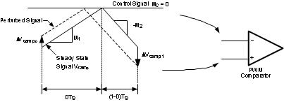
Current mode control has an inherent instability for duty cycles greater than 50%, as shown in Figure 6-3, where the control signal slope, MC, equals zero. In Figure 6-3, a small increase in the load current causes the sampled signal to increase by ΔVsamp0. The effect of this load change, ΔVsamp1, at the end of the first switching cycle is :

From Equation 9, when D > 0.5, ΔVsamp1 will be greater than ΔVsamp0. In other words, the disturbance is divergent. So a very small perturbation in the load will cause the disturbance to increase. To ensure that the perturbed signal converges we must maintain:

 Figure 6-3 Subharmonic Oscillation for D>0.5
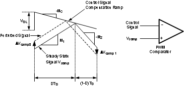
 Figure 6-4 Compensation Ramp Avoids Subharmonic Oscillation
To prevent the subharmonic oscillations, a compensation ramp is added to the control signal, as shown in Figure 6-4.
With the compensation ramp, ΔVsamp1 and the convergence criteria are expressed by,


The compensation ramp has been added internally in the LM3481. The slope of this compensation ramp has been selected to satisfy most applications, and its value depends on the switching frequency. This slope can be calculated using the formula:
In Equation 13, VSL is the amplitude of the internal compensation ramp and fS is the controller's switching frequency. Limits for VSL have been specified in the Section 5.5 section.
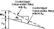
To provide the user additional flexibility, a patented scheme has been implemented inside the IC to increase the slope of the compensation ramp externally, if the need arises. Adding a single external resistor, RSL(as shown in Figure 6-6) increases the amplitude of the compensation ramp as shown in Figure 6-5.
 Figure 6-5 Additional Slope Compensation Added Using External Resistor RSL
Where,
K = 40 µA typically and changes slightly as the switching frequency changes. Figure 6-7 shows the effect the current K has on ΔVSLand different values of RSL as the switching frequency changes.
A more general equation for the slope compensation ramp, MC, is shown below to include ΔVSL caused by the resistor RSL.
It is good design practice to only add as much slope compensation as needed to avoid subharmonic oscillation. Additional slope compensation minimizes the influence of the sensed current in the control loop. With very large slope compensation the control loop characteristics are similar to a voltage mode regulator which compares the error voltage to a saw tooth waveform rather than the inductor current.
 Figure 6-6 Increasing the Slope of the Compensation Ramp
 Figure 6-7 ΔVSL vs RSL