SNVS346H November 2007 – October 2024 LM3481
PRODUCTION DATA
- 1
- 1 Features
- 2 Applications
- 3 Description
- 4 Pin Configuration and Functions
- 5 Specifications
- 6 Detailed Description
-
7 Application and Implementation
- 7.1 Application Information
- 7.2
Typical Applications
- 7.2.1
Boost Converter
- 7.2.1.1 Design Requirements
- 7.2.1.2
Detailed Design Procedure
- 7.2.1.2.1 Custom Design with WEBENCH Tools
- 7.2.1.2.2 Power Inductor Selection
- 7.2.1.2.3 Programming the Output Voltage and Output Current
- 7.2.1.2.4 Current Limit With Additional Slope Compensation
- 7.2.1.2.5 Power Diode Selection
- 7.2.1.2.6 Power MOSFET Selection
- 7.2.1.2.7 Input Capacitor Selection
- 7.2.1.2.8 Output Capacitor Selection
- 7.2.1.2.9 Driver Supply Capacitor Selection
- 7.2.1.2.10 Compensation
- 7.2.1.3 Application Curve
- 7.2.2 Typical SEPIC Converter
- 7.2.1
Boost Converter
- 7.3 Power Supply Recommendations
- 7.4 Layout
- 8 Device and Documentation Support
- 9 Revision History
- 10Mechanical, Packaging, and Orderable Information
Package Options
Mechanical Data (Package|Pins)
- DGS|10
Thermal pad, mechanical data (Package|Pins)
Orderable Information
7.4.1 Layout Guidelines
Good board layout is critical for switching controllers such as the LM3481. First the ground plane area must be sufficient for thermal dissipation purposes and second, appropriate guidelines must be followed to reduce the effects of switching noise. Switch mode converters are very fast switching devices. In such devices, the rapid increase of input current combined with the parasitic trace inductance generates unwanted Ldi/dt noise spikes. The magnitude of this noise tends to increase as the output current increases. This parasitic spike noise may turn into electromagnetic interference (EMI), and can also cause problems in device performance. Therefore, care must be taken in layout to minimize the effect of this switching noise. The current sensing circuit in current mode devices can be easily effected by switching noise. This noise can cause duty cycle jitter which leads to increased spectral noise. Although the LM3481 has 250-ns blanking time at the beginning of every cycle to ignore this noise, some noise may remain after the blanking time.
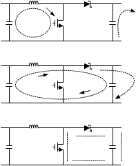
The most important layout rule is to keep the AC current loops as small as possible. Figure 7-9 shows the current flow of a boost converter. The top schematic shows a dotted line which represents the current flow during on-state and the middle schematic shows the current flow during off-state. The bottom schematic shows the currents we refer to as AC currents. These currents are the most critical currents because current is changing in very short time periods. The dotted lined traces of the bottom schematic are the once to make as short as possible.
 Figure 7-9 Current Flow in a Boost Application
The PGND and AGND pins have to be connected to the same ground very close to the device. To avoid ground loop currents attach all the grounds of the system only at one point.
A ceramic input capacitor should be connected as close as possible to the Vin pin and grounded close to the GND pin.
For a layout example please see AN-2094 LM3481 SEPIC Evaluation Board. For more information about layout in switch mode power supplies refer to AN-1229 SIMPLE SWITCHER® PCB Layout Guidelines.