SNVS346H November 2007 – October 2024 LM3481
PRODUCTION DATA
- 1
- 1 Features
- 2 Applications
- 3 Description
- 4 Pin Configuration and Functions
- 5 Specifications
- 6 Detailed Description
-
7 Application and Implementation
- 7.1 Application Information
- 7.2
Typical Applications
- 7.2.1
Boost Converter
- 7.2.1.1 Design Requirements
- 7.2.1.2
Detailed Design Procedure
- 7.2.1.2.1 Custom Design with WEBENCH Tools
- 7.2.1.2.2 Power Inductor Selection
- 7.2.1.2.3 Programming the Output Voltage and Output Current
- 7.2.1.2.4 Current Limit With Additional Slope Compensation
- 7.2.1.2.5 Power Diode Selection
- 7.2.1.2.6 Power MOSFET Selection
- 7.2.1.2.7 Input Capacitor Selection
- 7.2.1.2.8 Output Capacitor Selection
- 7.2.1.2.9 Driver Supply Capacitor Selection
- 7.2.1.2.10 Compensation
- 7.2.1.3 Application Curve
- 7.2.2 Typical SEPIC Converter
- 7.2.1
Boost Converter
- 7.3 Power Supply Recommendations
- 7.4 Layout
- 8 Device and Documentation Support
- 9 Revision History
- 10Mechanical, Packaging, and Orderable Information
Package Options
Mechanical Data (Package|Pins)
- DGS|10
Thermal pad, mechanical data (Package|Pins)
Orderable Information
7.2.1.2.2 Power Inductor Selection
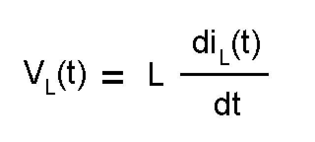
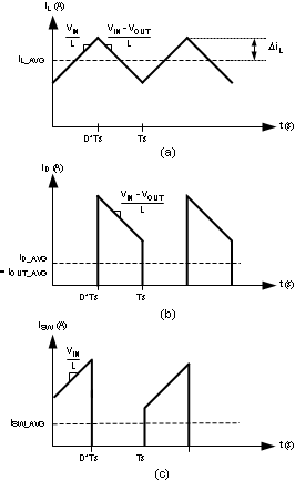
The inductor is one of the two energy storage elements in a boost converter. Figure 7-3 shows how the inductor current varies during a switching cycle. The current through an inductor is quantified as:

 Figure 7-3 (a) Inductor Current (b) Diode Current (c) Switch Current
If VL(t) is constant, diL(t)/dt must be constant. Hence, for a given input voltage and output voltage, the current in the inductor changes at a constant rate.
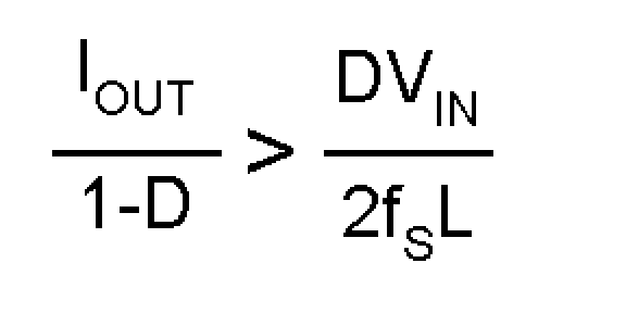
The important quantities in determining a proper inductance value are IL (the average inductor current) and ΔiL (the inductor current ripple difference between the peak inductor current and the average inductor current). If ΔiL is larger than IL, the inductor current drops to zero for a portion of the cycle and the converter operates in discontinuous conduction mode. If ΔiL is smaller than IL, the inductor current stays above zero and the converter operates in continuous conduction mode. All the analysis in this data sheet assumes operation in continuous conduction mode. To operate in continuous conduction mode, the following conditions must be met:


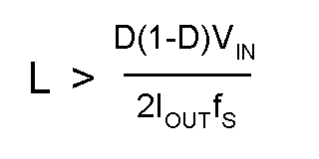
Choose the minimum IOUT to determine the minimum L. A common choice is to set (2 x ΔiL) to 30% of IL. Choosing an appropriate core size for the inductor involves calculating the average and peak currents expected through the inductor. In a boost converter,


A core size with ratings higher than these values should be chosen. If the core is not properly rated, saturation will dramatically reduce overall efficiency.
The LM3481 can be set to switch at very high frequencies. When the switching frequency is high, the converter can operate with very small inductor values. With a small inductor value, the peak inductor current can be extremely higher than the output currents, especially under light load conditions.
The LM3481 senses the peak current through the switch. The peak current through the switch is the same as the peak current calculated above.